CY7C143-35JI 查看數據表(PDF) - Cypress Semiconductor
零件编号
产品描述 (功能)
比赛名单
CY7C143-35JI Datasheet PDF : 13 Pages
| |||
CY7C133
CY7C143
Maximum Ratings
(Above which the useful life may be impaired. For user guide-
lines, not tested.)
Storage Temperature ..................................... −65°C to +150°C
Ambient Temperature with
Power Applied.................................................. −55°C to +125°C
Supply Voltage to Ground Potential
(Pin 48 to Pin 24).................................................−0.5V to +7.0V
DC Voltage Applied to Outputs
in High-Z State .....................................................−0.5V to +7.0V
DC Input Voltage ................................................. −3.5V to +7.0V
Output Current into Outputs (LOW)............................. 20 mA
Static Discharge Voltage........................................... >2001V
(per MIL-STD-883, Method 3015)
Latch-up Current..................................................... >200 mA
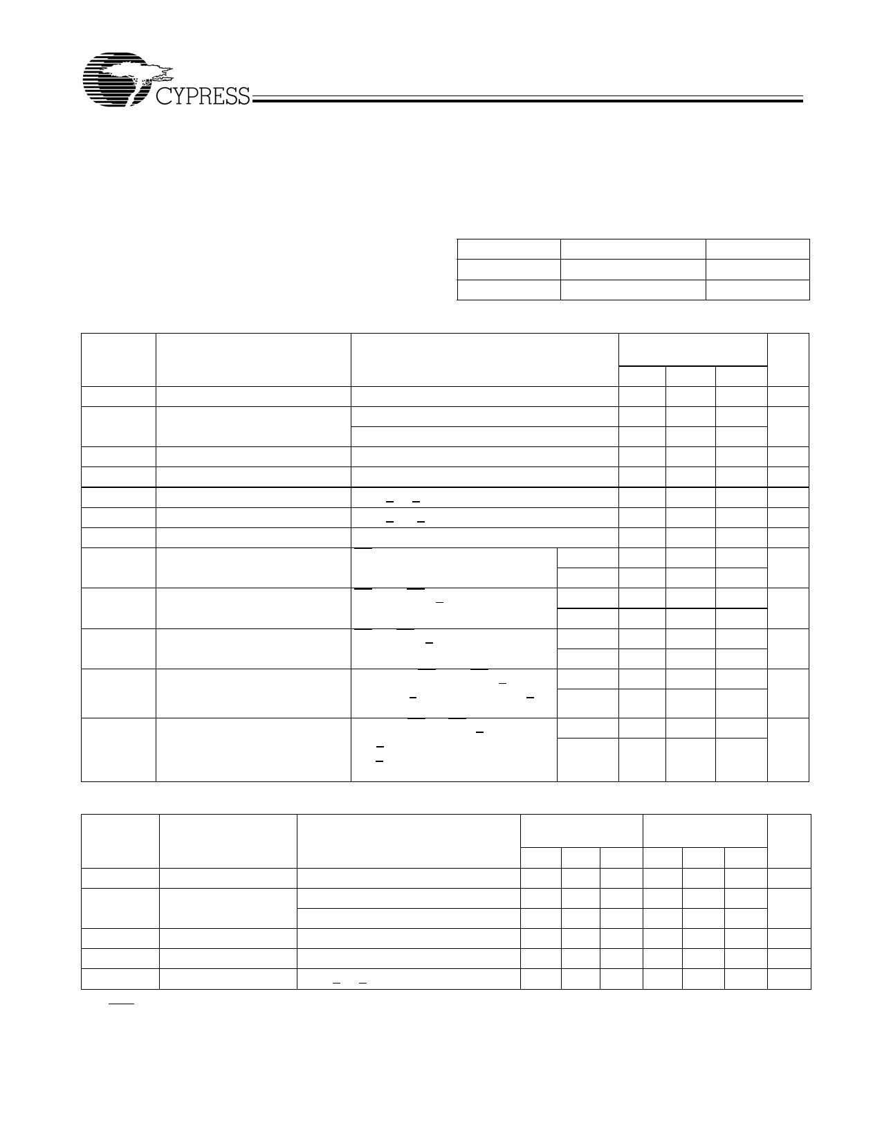
Operating Range
Range
Commercial
Industrial
Ambient Temperature
0°C to +70°C
−40°C to +85°C
VCC
5V ± 10%
5V ± 10%
Electrical Characteristics Over the Operating Range
Parameter
Description
Test Conditions
VOH
Output HIGH Voltage
VCC = Min., IOH = –4.0 mA
VOL
Output LOW Voltage
IOL = 4.0 mA
IOL = 16.0 mA[5]
VIH
Input HIGH Voltage
VIL
Input LOW Voltage
IIX
Input Leakage Current
GND < VI < VCC
IOZ
Output Leakage Current
GND < VO < VCC, Output Disabled
IOS
Output Short Circuit Current[6,7] VCC = Max., VOUT = GND
ICC
VCC Operating Supply Current
CE = VIL,
Outputs Open,
f
=
fMAX[8]
Com’l
Ind.
ISB1
Standby Current Both Ports, TTL CEL and CER > VIH, f = fMAX[8]
Com’l
Inputs
Ind.
ISB2
Standby Current One Port, TTL
Inputs
COEutLpourtsCOEpRe>n,VfIH=,fAMcAtXiv[8e] Port
Com’l
Ind.
ISB3
Standby Current Both Ports,
Both Ports CEL and CER > VCC – Com’l
CMOS Inputs
0.2V, VIN > VCC – 0.2V or VIN < Ind.
0.2V, f = 0
ISB4
Standby Current One Port,
One Port CEL or CER > VCC – 0.2V, Com’l
CMOS Inputs
VIN > VCC – 0.2V or
Vf =INfM<A0X.[82]V, Active Port Outputs Open,
Ind.
7C133-25
7C143-25
Min. Typ. Max. Unit
2.4
V
0.4
V
0.5
2.2
V
0.8
V
−5
+5 µA
−5
+5 µA
−200 mA
170 250 mA
170 290
40
60 mA
40
75
100 140 mA
100 160
3
15 mA
3
15
90 120 mA
90 140
Electrical Characteristics Over the Operating Range (continued)
7C133-35
7C143-35
7C133-55
7C143-55
Parameter
Description
Test Conditions
Min. Typ. Max. Min. Typ. Max. Unit
VOH
Output HIGH Voltage VCC = Min., IOH = –4.0 mA
2.4
2.4
V
VOL
Output LOW Voltage IOL = 4.0 mA
IOL = 16.0 mA[5]
0.4
0.4 V
0.5
0.5
VIH
Input HIGH Voltage
2.2
2.2
V
VIL
Input LOW Voltage
0.8
0.8 V
IIX
Input Leakage Current GND < VI < VCC
−5
+5 −5
+5 µA
Notes:
5. BUSY pin only.
6. Duration of the short circuit should not exceed 30 seconds.
7. Tested initially and after any design or process changes that may affect these parameters.
8. At f=fMAX, address and data inputs are cycling at the maximum frequency of read cycle of 1/tRC and using AC Test Waveforms input levels of GND to 3V.
Document #: 38-06036 Rev. *B
Page 5 of 13
Share Link: 