P80C557E6 查看數據表(PDF) - Philips Electronics
零件编号
产品描述 (功能)
比赛名单
P80C557E6 Datasheet PDF : 64 Pages
| |||
Philips Semiconductors
Single-chip 8-bit microcontroller
Product specification
P83C557E6/P80C557E6
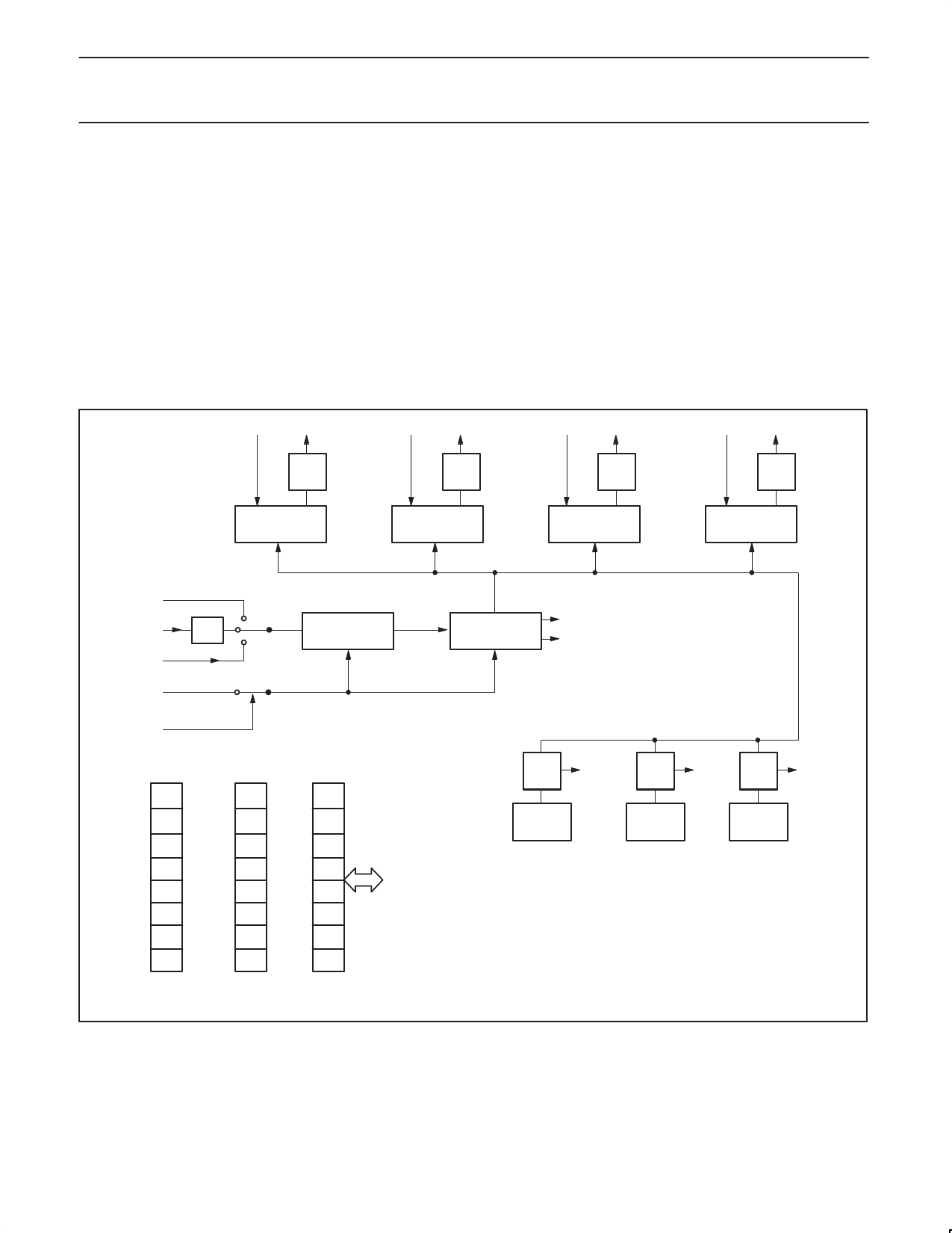
6.7.2 Timer T2
Timer T2 is a 16 bit timer/counter which has capture and compare
facilities. The operational diagram is shown in Figure 21.
The 16 bit timer/counter is clocked via a prescaler with a
programmable division factor of 1, 2, 4 or 8. The input of the
prescaler is clocked with 1/12 of the clock frequency, or by an
external source connected to the T2 input, or it is switched off. The
maximum repetition rate of the external clock source is fCLK/12,
twice that of Timer 0 and Timer 1. The prescaler is incremented on a
rising edge. It is cleared if its division factor or its input source is
changed, or if the timer/counter is reset (see also Figure 22:
TM2CON). T2 is readable ‘on the fly’, without any extra read
latches; this means that software precautions have to be taken
against misinterpretation at overflow from least to most significant
byte while T2 is being read. T2 is not loadable and is reset by the
RST signal or at the positive edge of the input signal RT2, if
enabled. In the Idle or Power-down Mode the timer/counter and
prescaler are reset and halted.
T2 is connected to four 16-bit Capture Registers: CT0, CT1, CT2
and CT3. A rising or falling edge on the inputs CT0I, CT1I, CT2I or
CT3I (alternative function of Port 1) results in loading the contents of
T2 into the respective Capture Registers and an interrupt request.
Using the Capture Register CTCON (see Figure 23), these inputs
may invoke capture and interrupt request on a positive, a negative
edge or on both edges. If neither a positive nor a negative edge is
selected for capture input, no capture or interrupt request can be
generated by this input.
CT0I
INT
CT1I
INT
CT2I
INT
CT3I
INT
CTI0
CTI1
CTI2
CTI3
CT0
CT1
CT2
CT3
off
fCLK
1/12
T2
RT2
T2ER
External reset
enable
S
R
S
R
S
R
S
R
S
R
S
R
TG
T
TG
T
STE
RTE
Prescaler
T2 Counter
8-bit overflow interrupt
16-bit overflow interrupt
P4.0
P4.1
P4.2
P4.3
P4.4
P4.5
P4.6
P4.7
I/O port 4
COMP
INT
COMP
INT
COMP
INT
CMO (S)
CM1 (R)
CM2 (T)
S = set
R = reset
T = toggle
TG = toggle status
T2 SFR address: TML2 = lower 8 bits
TMH2 = higher 8 bits
Figure 21. Block diagram of Timer 2.
1999 Mar 02
24
Share Link: 