P80C557E6 查看數據表(PDF) - Philips Electronics
零件编号
产品描述 (功能)
比赛名单
P80C557E6 Datasheet PDF : 64 Pages
| |||
Philips Semiconductors
Single-chip 8-bit microcontroller
Product specification
P83C557E6/P80C557E6
6.9.2 SIO1 (I2C-bus Interface)
The SIO1 of the P8xC557E6 provides the fast–mode, which allows
a fourthfold increase of the bitrate up to 400 kHz. Nevertheless it is
downward compatible, i.e. it can be used in a 0 to 100 Kbit/s I2C bus
system.
Except from the bit rate selection (see Table 25) and the timing of
the SCL and SDA signals (see AC electrical characteristics in
section 11) the SIO circuit is the same as described in detail in the
80C51 Data Handbook IC20 for the 8xC552 microcontroller.
The I2C–bus is a simple bidirectional 2–wire bus for efficient inter–IC
data exchange. Features of the I2C–bus are:
• Only two bus lines are required: a serial clock line (SCL) and a
serial data line (SDA)
• Each device connected to the bus is software addressable by a
unique address
• Masters can operate as Master–transmitter or as Master–receiver
• It’s a true multi–master bus including collision detection and
arbitration to prevent data corruption if two or more masters
simultaneously initiate data transfer
• Serial clock synchronization allows devices with different bit rates
to communicate via the same serial bus
• ICs can be added to or removed from an I2C–bus system without
affecting any other circuit on the bus
• Fault diagnostics and debugging are simple; malfunctions can be
immediately traced
For more information on the I2C–bus specification (including
fast–mode) please refer to the Philips publication number 9398 393
40011 and/or the 80C51 Data Handbook IC20.
The on–chip I2C logic provides a serial interface that meets the
I2C–bus specification, supporting all I2C–bus modes of operation,
they are:
• Master transmitter
• Master receiver
• Slave transmitter
• Slave receiver
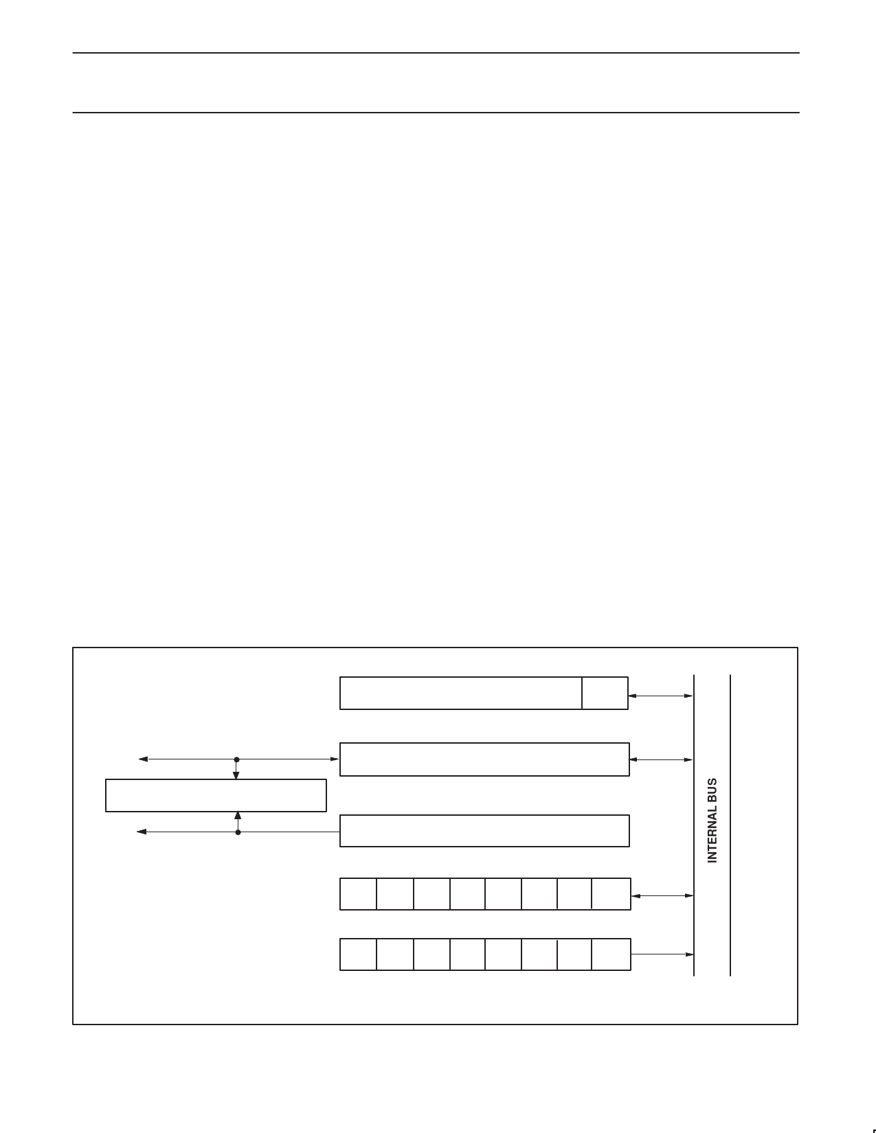
The SI01 logic performs a byte oriented data transport, clock
generation, address recognition and bus control arbitration are all
controlled by hardware. Via two pins the external I2C–bus is
interfaced to the SIO1 logic: SCL serial clock I/O and SDA serial
data I/O, (see Special Function Register bit S1CON.6/ENS1 for
enabling the SIO1 logic).
The SIO1 logic handles byte transfer autonomously. It keeps track of
the serial transfers, and a status register (S1STA) reflects the status
of SIO1 and the I2C–bus.
Via the following four Special Function Registers the CPU interfaces
to the I2C logic.
S1CON control register. Bit addressable by the CPU
S1STA status register whose contents may be used as a vector to
service routines.
S1DAT data shift register. The data byte is stable as long as
S1CON.3/SI=1.
S1ADR slave address register. It’s LSB enables/ disables general
call address recognition.
SDA
ARBITRATION + SYNC LOGIC
SCL
7
S1ADR
7
S1DAT
SLAVE ADDRESS
1
0
GC
0
SHIFT REGISTER
BUS CLOCK GENERATOR
7
0
S1CON
7
0
S1STA
Figure 29. Block diagram of I2C serial I/O interface.
1999 Mar 02
30
Share Link: 