SAB-C505C-4E 查看數據表(PDF) - Infineon Technologies
零件编号
产品描述 (功能)
比赛名单
SAB-C505C-4E Datasheet PDF : 88 Pages
| |||
C505 / C505C
C505A / C505CA
Table 2
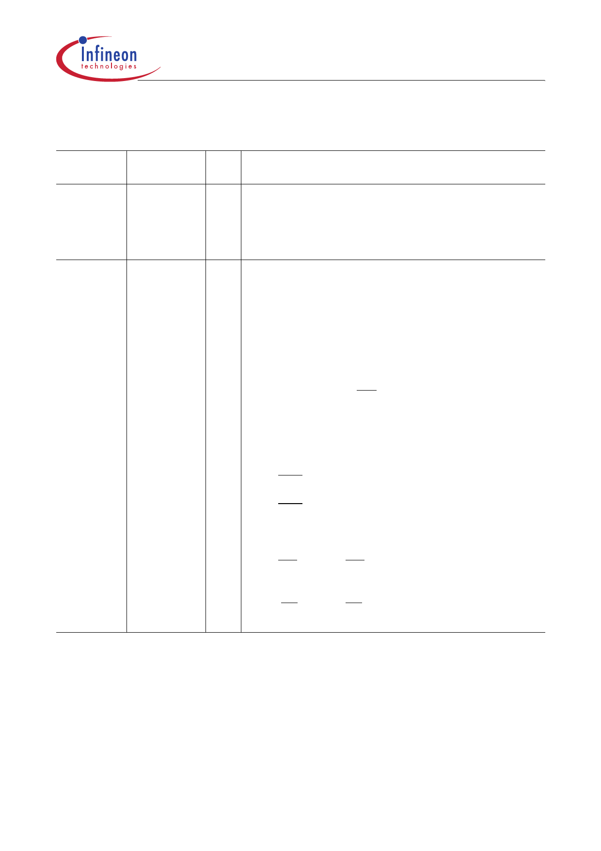
Pin Definitions and Functions
Symbol
RESET
Pin Number I/O
*)
4
I
P3.0-P3.7 5, 7-13
I/O
5
7
8
9
10
11
12
13
*) I = Input
O = Output
Function
RESET
A high level on this pin for two machine cycle while the
oscillator is running resets the device. An internal diffused
resistor to VSS permits power-on reset using only an
external capacitor to VDD.
Port 3
is an 8-bit quasi-bidirectional port with internal pull-up
arrangement. Port 3 pins that have 1’s written to them are
pulled high by the internal pull-up transistors and in that
state can be used as inputs. As inputs, port 3 pins being
externally pulled low will source current (IIL, in the DC
characteristics) because of the internal pullup transistors.
The output latch corresponding to a secondary function
must be programmed to a one (1) for that function to operate
(except for TxD and WR). The secondary functions are
assigned to the pins of port 3 as follows:
P3.0 / RxD
Receiver data input (asynch.) or data
input/output (synch.) of serial interface
P3.1 / TxD
Transmitter data output (asynch.) or
clock output (synch.) of serial interface
P3.2 / INT0
External interrupt 0 input / timer 0 gate
control input
P3.3 / INT1
External interrupt 1 input / timer 1 gate
control input
P3.4 / T0
Timer 0 counter input
P3.5 / T1
Timer 1 counter input
P3.6 / WR
WR control output; latches the data
byte from port 0 into the external data
memory
P3.7 / RD
RD control output; enables the external
data memory
Data Sheet
7
08.00
Share Link: 