CXP86609 查看數據表(PDF) - Sony Semiconductor
零件编号
产品描述 (功能)
比赛名单
CXP86609 Datasheet PDF : 20 Pages
| |||
CXP86609/86613/86617
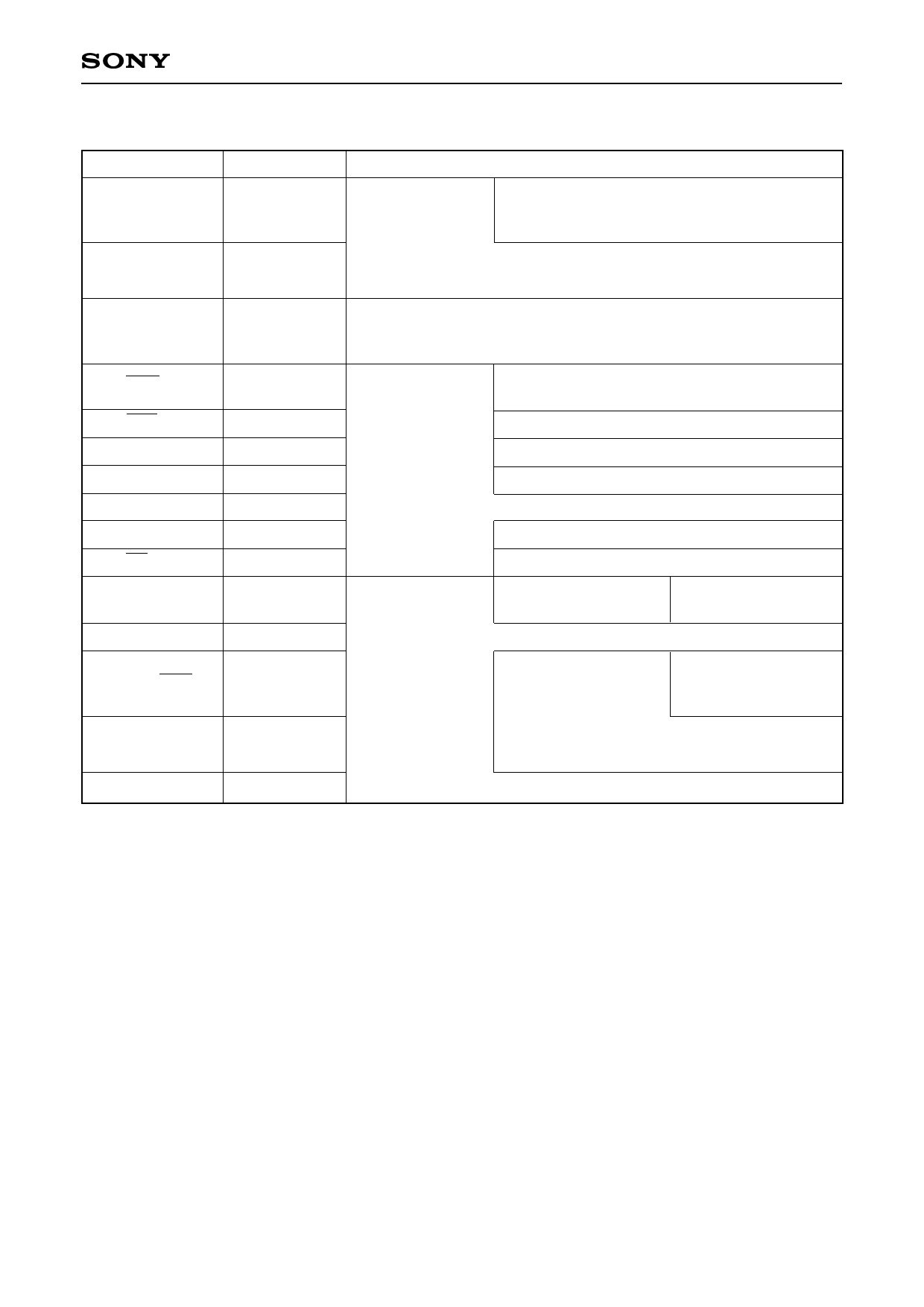
Pin Description
Symbol
PA0/AN0
to
PA5/AN5
PA6 to PA7
PB0 to PB7
PD0/INT2
PD1/SCK
PD2/SO
PD3/SI
PD4 to PD5
PD6/RMC
PD7/EC
PE0/TO/ADJ
PE1
PE2/TEX/INT0
PE3/TX
PE4 to PE6
I/O
I/O/
Analog input
I/O
I/O
I/O/Input
I/O/I/O
I/O/Output
I/O/Input
I/O
I/O/Input
I/O/Input
I/O/Output/
Output
I/O
Input/Input/
Input
Input/Output
Output
Description
(Port A)
8-bit I/O port.
I/O can be set in
a unit of single bits.
(8 pins)
Analog inputs to A/D converter.
(6 pins)
(Port B)
8-bit I/O port. I/O can be set in a unit of single bits.
(8 pins)
(Port D)
8-bit I/O port.
I/O can be set in
a unit of single bits.
Can drive 12mA
sink current.
(8 pins)
External interruption request input.
Active at the falling edge.
Serial clock I/O.
Serial data output.
Serial data input.
Remote control reception circuit input.
(Port E)
Bits 0 and 1 are
I/O port; I/O can
be set in a unit of
single. Bits 2 and 3
are input port.
Bits 4, 5 and 6 are
output port.
(7 pins)
External event input for timer/counter.
Rectangular wave output 32kHz oscillation
for 8-bit timer/counter. frequency dividing output.
Connects a crystal for External interruption
32kHz timer/counter request input. Active at
clock oscillation.
the falling edge.
When used as an event
counter, input to TEX pin
and leave TX pin open.
–4–
Share Link: 