AN-6920MR 查看數據表(PDF) - Fairchild Semiconductor
零件编号
产品描述 (功能)
比赛名单
AN-6920MR
Fairchild Semiconductor

AN-6920MR Datasheet PDF : 17 Pages
| |||
AN-6920
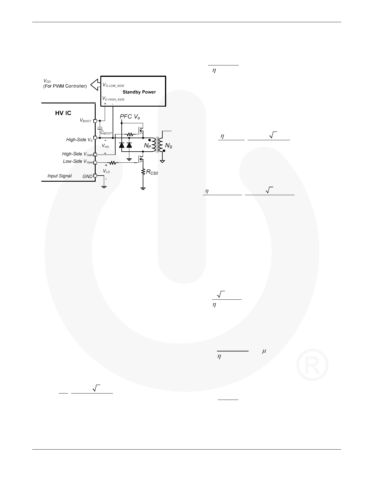
Figure 9 shows the high-side driver circuit with standby
power supply. This circuit uses the independent power
supply for HV IC to keep the high-side driver operating.
This circuit is used for applications with standby power, like
the PC power.
Figure 9. High-Side Driver Circuit with Standby
Power Supply
5. Design Considerations
This design procedure uses the schematic in Figure 1 as a
reference. A 90W PFC application with universal input
range is selected as a design example. The design
specifications are:
- Line Voltage Range: 90~264VAC (60Hz)
- Output of DC/DC Converter: 19V/4.7A (90W)
- PFC Output Voltage: 400V
- Minimum PFC Switching Frequency: > 50kHz
- Brownout Protection Line Voltage: 70VAC
- Output Over-Voltage Protection Trip Point: 22.5V
- Overall Efficiency: 90%
(PFC Stage: 95%, DC/DC Stage: 95%)
Part A. PFC Section
[STEP-A1] Boost Inductor Design
The boost inductor value is determined by the output power
and the minimum switching frequency. From Equation 2,
the minimum frequency with a given line voltage and
MOSFET on time is obtained as:
fSW ,MIN
=
1
tON
⋅ VO.PFC − 2VLINE
VO.PFC
(3)
where:
VLINE is RMS line voltage;
tON is the MOSFET conduction time; and
VO.PFC is the PFC output voltage.
APPLICATION NOTE
The MOSFET conduction time with a given line voltage at a
nominal output power is given as:
tON
=
2 ⋅ PO.PFC ⋅ L
η ⋅VLINE 2
(4)
where:
η is the overall efficiency;
L is the boost inductance; and
POUT is the nominal output power.
Using Equation 4, the minimum switching frequency of
Equation 3 can be expressed as:
fSW ,MIN
=
η ⋅VLINE2 ⋅ VO.PFC − 2VLINE
2 ⋅ POUT ⋅ L
VO.PFC
(5)
Since the minimum frequency occurs at high line as long as
the PFC output voltage is lower than 405V (as observed in
Figure 5); once the output voltage and minimum switching
frequency are set, the inductor value is given as:
L = η ⋅ (VLINE.MAX )2 ⋅ VO.PFC − 2VLINE.MAX
(6)
2 ⋅ POUT ⋅ fSW ,MIN
VO.PFC
where VLINE,MAX is the maximum line voltage.
As the minimum frequency decreases, the switching loss is
reduced, while the inductor size and line filter size increase.
Thus, the minimum switching frequency should be
determined by the trade-off between efficiency and the size
of magnetic components. The minimum switching
frequency must be above 20kHz to prevent audible noise.
Once the inductance value is decided, the maximum peak
inductor current at the nominal output power is obtained at
low-line condition as:
I L.PK
2
=
2 ⋅ POUT
η ⋅VLINE,MIN
(7)
where VLINE,MIN is the minimum line voltage.
Since the maximum on time is internally limited at 20µs, it
should be smaller than 20µs such as:
t MAX
ON
= 2 ⋅ POUT ⋅ L
η ⋅VLINE.MIN 2
< 20µs
(8)
The number of turns of boost inductor should be determined
considering the core saturation. The minimum number is
given as:
NBOOST
≥
IL,PK ⋅ L
Ae ⋅ ∆B
(9)
where is Ae is the cross-sectional area of core and ∆B is the
maximum flux swing of the core in Tesla.
∆B should be set below the saturation flux density.
© 2010 Fairchild Semiconductor Corporation
Rev. 1.0.0 • March 10, 2011
5
www.fairchildsemi.com
Share Link: