HTG13J0 查看數據表(PDF) - Holtek Semiconductor
零件编号
产品描述 (功能)
比赛名单
HTG13J0 Datasheet PDF : 30 Pages
| |||
HT13J0
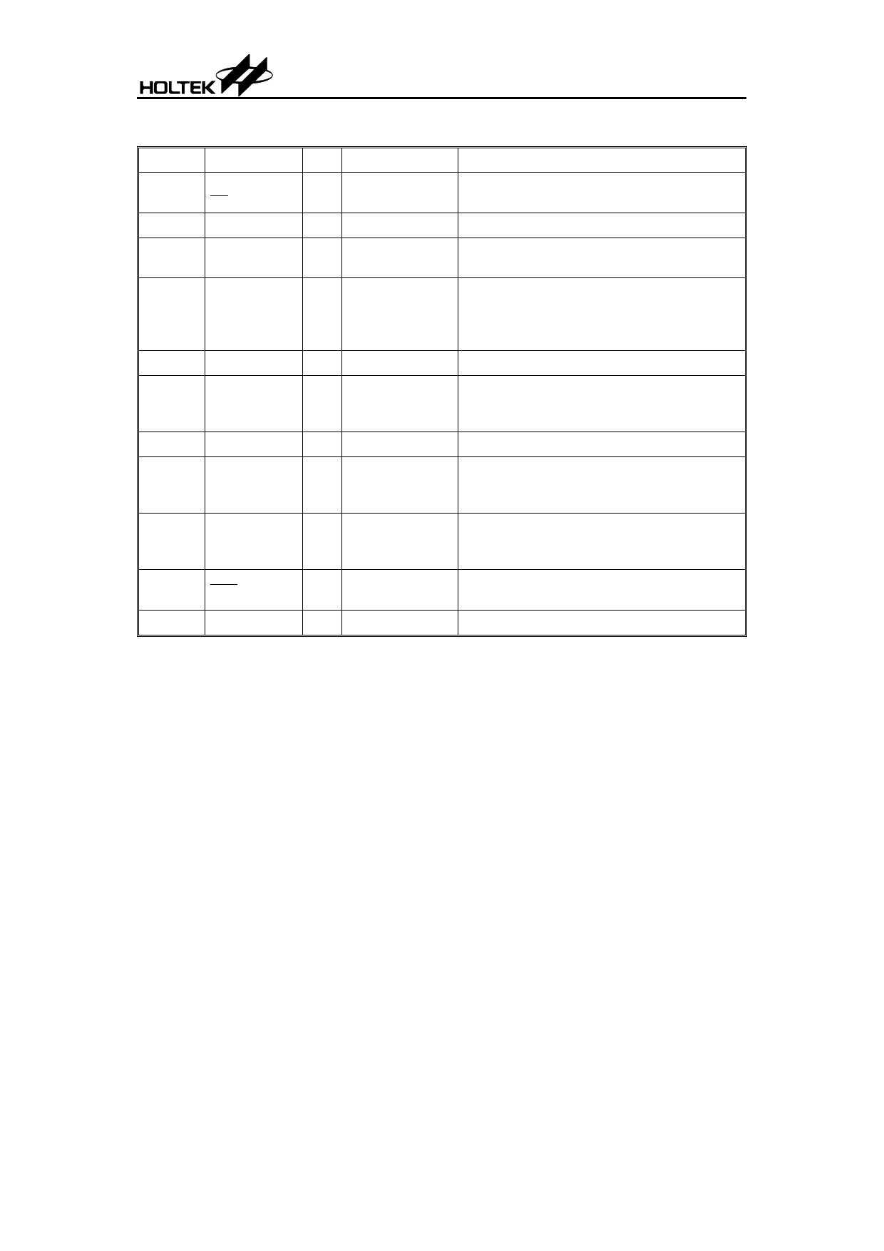
Pad Description
Pad No. Pad name I/O
1
BZ
2
BZ
O
3
VDD
I
4
OSCI
I
5
OSCO
O
6
T512
O
15
TEST1
I
16
TEST2
I
21
T1D
O
7~14
COM7~COM0 O
17~19
22
PS2~PS0
PS3
I
20
VSS
I
23~25 PA2~PA0
O
26~29 PP0~PP3
I
30
31~70
RES
I
SEG39~SEG0 O
Mask Option
Description
*
Sound effect output
¾
¾
¾
¾
Pull-high or
None
**
¾
CMOS or
NMOS
Open Drain
Pull-high or
None
**
¾
¾
Positive power supply
OSCI, OSCO are connected to resistor for in-
ternal system clock.
For test mode only
TEST1 and TEST2 must be open when the
chip is in normal operation (with internal pull
high resistor).
Output for LCD panel common plate
4-bit port for input only
Negative power supply, GND
3-bit latch port for output only
4-bit port for input only
Input to reset LSI
Reset is active at logical low level.
LCD driver outputs for LCD panel segment
*: 6 internal sources deriving from system clock can be selected as sound effect clock by mask op-
tion. If Holtek s sound library is invoked, only 128K and 64K is accepted.
**: Each bit of input ports PS, PP can be a trigger source of HALT interrupt. That can be specified
by mask option.
Absolute Maximum Ratings
Supply Voltage .............................-0.3V to 5.5V
Input Voltage ................VSS-0.3V to VDD+0.3V
Storage Temperature ................-50°C to 125°C
Operating Temperature ..................0°C to 70°C
Note: These are stress ratings only. Stresses exceeding the range specified under "Absolute Maxi-
mum Ratings" may cause substantial damage to the device. Functional operation of this device
at other conditions beyond those listed in the specification is not implied and prolonged expo-
sure to extreme conditions may affect device reliability.
5
May 19, 1999
Share Link: 