HTG13J0 查看數據表(PDF) - Holtek Semiconductor
零件编号
产品描述 (功能)
比赛名单
HTG13J0 Datasheet PDF : 30 Pages
| |||
Program memory - ROM
The program memory is used to store program
instruction which is to be executed. It is orga-
nized with 8192 ´ 8 bits and addressed by the
program counter and PA3.
Certain locations in bank 0 of the program
memory are reserved for specific usage:
· Location 0004H
This area are reserved for TIMER interrupt
service program. A timer interrupt resulting
from TIMER overflow, if interrupt is enabled
the CPU begins execution at location 0004H.
· Location 0008H
Activating the PS or PP input pins of the pro-
cessor with the interrupts enabled during
HALT mode causes the program to jump to
this location.
· Location 0n00H~0nFFH (n=current number)
and 0F00H~0FFFH.
The last 256 bytes of each page in the pro-
gram memory, addressed from 0n00H to
0nFFH and 0F00H to 0FFFH can be used as a
look up table. The instructions READ R4A,
READ MR0A, READF R4A, READF MR0A
can read the table and transfer the contents of
the table to ACC and R4 or transfer to ACC
and data memory addressed by register pair
R1,R0 . These area may function as normal
program memory depending on the require-
ment. Note that the page number n must be
greater than zero, some locations in page 0
are reserved for specific usage as mentioned.
Certain locations in bank 1 of the program
memory are reserved for specific usage:
· Location 1000H
This area are reserved for the initialization
program. After reset, the CPU always begins
execution at location 1000H.
· Location 1004H
This area is reserved for TIMER interrupt
service program. A timer interrupt resulting
from TIMER overflow, if interrupt is enabled,
the CPU begins execution at location 1004H.
HT13J0
· Location 1008H
Activating the PS or PP input pins of the pro-
cessor with the interrupts enabled during
HALT mode causes the program to jump to
this location.
· Location 1n00H~1nFFH (n=current number)
and 1F00H~1FFFH.
The last 256 bytes of each page in the pro-
gram memory, addressed from 1n00H to
1nFFH and 1F00H to 1FFFH can be used as a
loop up table. The instructions READ R4A,
READ MR0A, READF R4A, READF MR0A
can read the table and transfer the contents of
the table to ACC and R4 or transfer to ACC
and data memory addressed by register pair
"R1,R0" These area may function as normal
program memory depending on the require-
ment. Note that the page number n must be
greater than zero, some locations in page 1
are reserved for specific usage as mentioned.
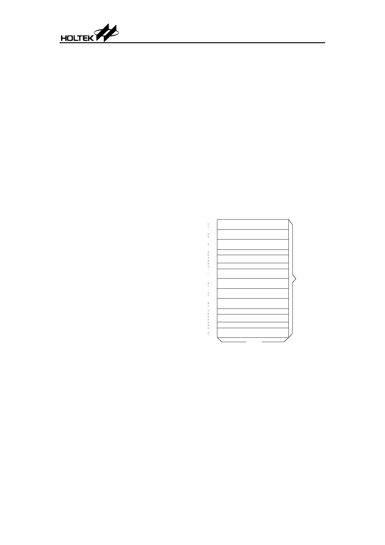
The program memory (ROM) mapping is shown
below:
0000H
0003H
0004H
0007H
0008H
000BH
Timer interrupt subroutine of bank 0
External interrupt subroutine of bank 0
Page n look-up table (256 bytes) of bank 0
0F00H
0FFFH
1000H
1003H
1004H
1007H
1008H
100BH
Page F look-up table (256 bytes) of bank 0
Reset initial program
Timer interrupt subroutine of bank 1
External interrupt subroutine of bank 1
Page look-up table (256 bytes) of bank 1
1F00H
1FFFH
Page F look-up table (256 bytes) of bank 1
8 bits
Program memory
Program ROM
9
May 19, 1999
Share Link: 