HSP-EVAL 查看數據表(PDF) - Intersil
零件编号
产品描述 (功能)
比赛名单
HSP-EVAL Datasheet PDF : 12 Pages
| |||
HSP-EVAL
As an example, consider the loading of the least significant
byte of the “Logical” Input Register, Input Register 1, as
shown by the Timing Diagram in Figure 2. First, data is down
loaded to the Parallel Port Interface's Holding Register. Next,
the address register is written with a value which contains
the address of the LSB Register for Input Register 1 (see
Table 7 for memory map), the HSP-EVAL board address
(assumed to be zero in this example), and a “high” in the LD
bit position (see Table 9 for Address Register Bit Map).
Finally, data is latched into the targeted register by rewriting
the address register with the same board and register
address but with a “low” in the LD bit position. The “high/low”
transition of the LD bit loads the data in the holding register
into the target data register on the specified HSP-EVAL.
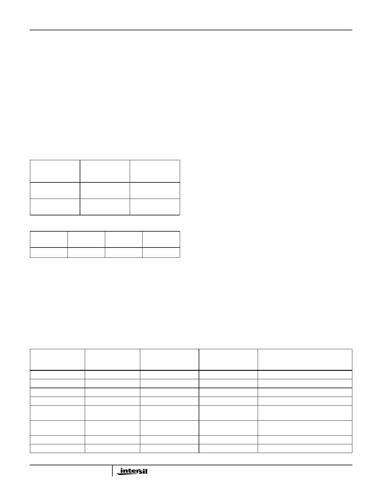
TABLE 7. SHIFT REGISTER TO OUTPUT BUS MAPPINGS
SHIFT REGISTER REGISTER TO BUS
BITS
SIGNAL MAPPING
(MSBIT-LSBIT)
(MSBIT-LSBIT)
DESCRIPTION
15-0
OUT2_15-0
DATA ON OUTPUT
BUS 2
31-16
OUT1_31-16
DATA ON OUTPUT
BUS 1
TABLE 8. ADDRESS REGISTER BIT MAP
NOT USED
LD BIT
BOARD
ADDRESS
REGISTER
ADDRESS
D7
D6
D5-3
D2-0
Up Loading Data via PC's Parallel Port
Data is up loaded to the host PC through the “Busy”, “Paper
End”, and “Select” status lines of the PC's parallel port. The
PC up loads data by monitoring the state of the PCRD0-2
serial output lines on the HSP-EVAL's Parallel Port Bus. The
mapping of the parallel port status lines to the Parallel Port
Busses serial output lines is given in Table 6. The serial
output lines are driven by daughter board output and status
as specified by jumper placement in the J4 Configuration
Jumper Field.
By monitoring the Parallel Port Bus’s PCRD2 line, a PC up
loads data on the HSP_EVAL's output busses which has
been serialized by the Output Shift Register. The Shift
Register is loaded by a “low” to “high” transition on the CTL3
bit of the CTL Control Register. Once the Shift Register has
been loaded, data is clocked out by “low” to “high” transitions
on the CTL2 bit of the CTL Register. The timing relationship
between CTL2-3 for loading and clocking data out of the
Shift Register is shown in Figure 3. The data in the Shift
Register is output to the PCRD2 line of the HSP-EVAL's
Parallel Port Bus by inserting a jumper in the SR_RD
position of the J4 Configuration Jumper Field. The PCRD2
line is monitored by the “Paper End” status line of the PC's
parallel port.
The HSP-EVAL can be configured such that one of the four
Status Bus Lines STAT0-3 is selected for monitoring via the
PCRD0-1 lines of the Parallel Port Bus. To select one of the
Status Bus lines for output, a jumper is inserted in one of the
STAT0-3 positions of the J4 Jumper Configuration Field.
The selected status line drives a flip-flop which is configured
to function as an R/S latch (see U17, page 2, of the
schematics). A “low” state on the selected status line sets
the output of the flip-flop “high” when the CTL1 bit of the CTL
Control Register is “high”. The output of the latch remains
”high” until it is reset by forcing the CTL1 bit “low” while the
status input is “high”. This structure is used to capture the
occurrence of a “low” state on a status line which is normally
“high”. The output of the flip-flop drives either the PCRD0 or
PCRD1 lines of the Parallel Port Bus by placing a jumper at
either the PCRD0 or PCRD1 positions in the J4
Configuration Jumper Field.
REGISTER ADDRESS
0
1
2
3
4
5
6
7
TABLE 9. REGISTER TO INPUT/CONTROL BUS MAPPINGS
REGISTER BITS
(MSB-LSB)
REGISTER TO BUS
SIGNAL MAPPING
(MSB-LSB)
REGISTER TO
CONNECTOR
MAPPING
LOGICAL REGISTER
MAPPING
7-0
IN3_7-0
J3
INPUT REGISTER 3 (LSBYTE)
7-0
IN3_15-8
J3
INPUT REGISTER 3 (MSBYTE)
7-0
IN2_7-0
J1
INPUT REGISTER 2 (LSBYTE)
7-0
IN2_15-8
J1
INPUT REGISTER 2 (MSBYTE)
7-0
CTL7-0
J3
CTL CONTROL REGISTER
(LSBYTE)
7-0
CTL15-8
J3
CTL CONTROL REGISTER
(MSBYTE)
7-0
IN1_7-0
J1
INPUT REGISTER 1 (LSBYTE)
7-0
IN1_15-8
J1
INPUT REGISTER 1 (MSBYTE)
6
Share Link: 