HT7612B 查看數據表(PDF) - Holtek Semiconductor
零件编号
产品描述 (功能)
比赛名单
HT7612B Datasheet PDF : 20 Pages
| |||
HT7612/HT7612B
Absolute Maximum Ratings
Supply Voltage ...........................VSS-0.3V to VSS+6.0V
Input Voltage..............................VSS-0.3V to VDD+0.3V
Zero Crossing Current ................................Max. 300mA
Storage Temperature ............................-50°C to 125°C
Operating Temperature...........................-40°C to 85°C
Note: These are stress ratings only. Stresses exceeding the range specified under ²Absolute Maximum Ratings² may
cause substantial damage to the device. Functional operation of this device at other conditions beyond those listed
in the specification is not implied and prolonged exposure to extreme conditions may affect device reliability.
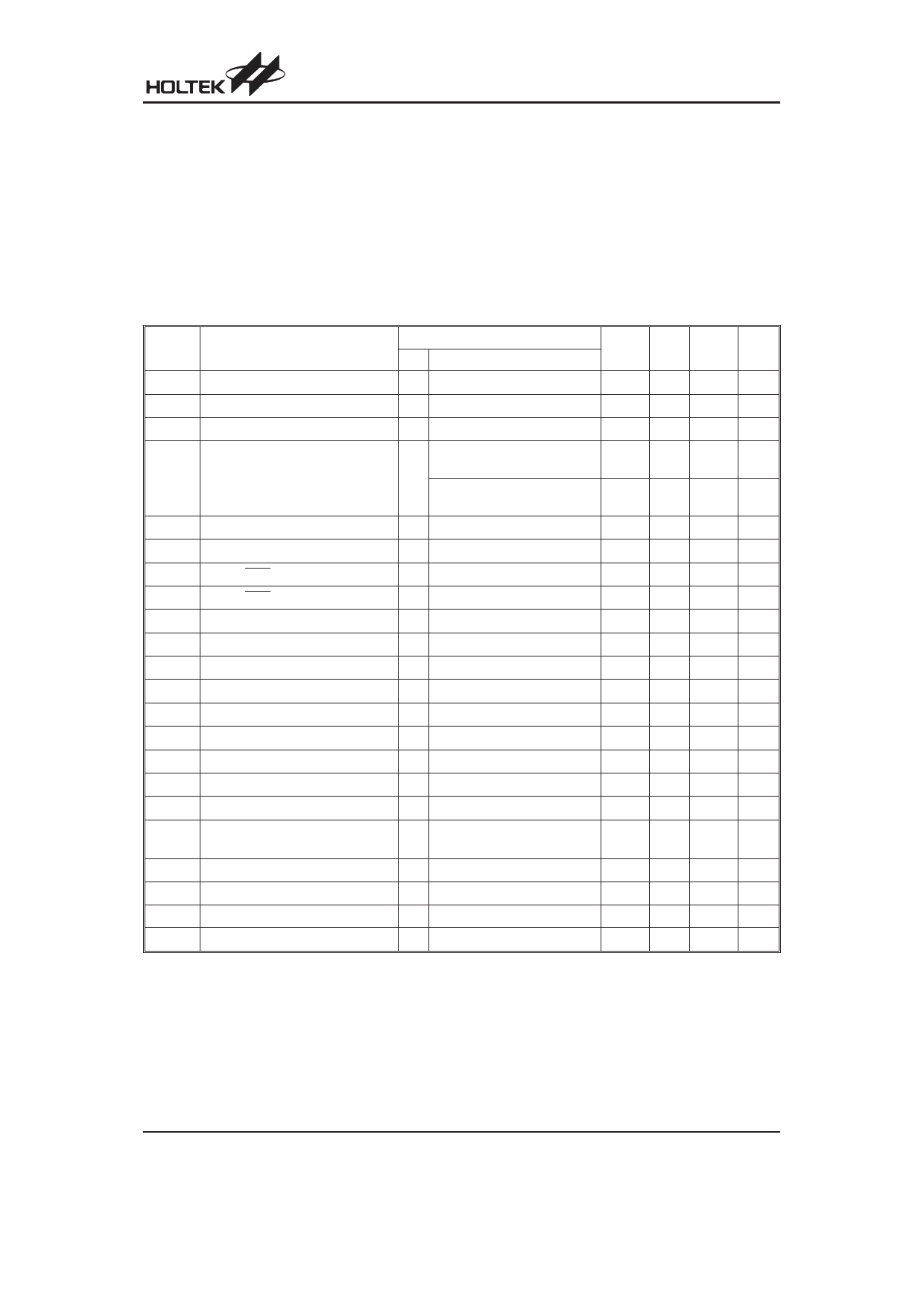
Electrical Characteristics
Ta=25°C
Symbol
Parameter
Test Conditions
VDD
Conditions
Min. Typ. Max. Unit
VDD
Operating Voltage
¾
¾
2.7 4.0 5.5 V
VREF Reference Voltage - see Note
5V Cf=1mF
3.201 3.300 3.399 V
IREF
Driving Current
5V
¾
200 ¾
¾
mA
ISTB
Standby Current
HT7612: DT off, OPAMP off,
VREF no load
¾
17
23
mA
5V
HT7612B: DT off, OPAMP on,
VREF no load
¾
19
25
mA
IOH1
TRIAC Source Current
5V VOH=4.5V
-20 -40 ¾ mA
IOL1
TRIAC Sink Current
5V VOL=0.5V
20
40
¾ mA
IOH2
BUZ & BUZ Source Current
5V VOH=4.5V
-5 -10 ¾ mA
IOL2
BUZ & BUZ Sink Current
5V VOL=0.5V
10
20
¾ mA
IOH3
RELAY/LED Source Current
5V VOH=4.5V
-5 -10 ¾ mA
IOL3
RELAY/LED Sink Current
5V VOL=0.5V
10
20
¾ mA
VIH
MODE High Input Voltage
¾
¾
0.7VDD ¾
¾
V
VIL
MODE Low Input Voltage
¾
¾
¾
¾ 0.3VDD V
VTH1 ZC High Transfer Voltage
¾
¾
0.7VDD ¾
¾
V
VTL1
ZC Low Transfer Voltage
¾
¾
¾
¾ 0.3VDD V
VOS
OP Amp Input Offset Voltage
5V CL=10pF
¾
10
¾ mV
VLVD Low Voltage Detector Voltage
¾
¾
0.99 1.10 1.21 V
fSYS
System Oscillator Frequency - IRC 5V
¾
28.8 32.0 35.2 kHz
fDT
Delay Time Frequency - ERC
¾
VREF, RDT=30kW,
CDT=3000pF
15.2 16.0 16.8 kHz
AVO OP Amp Open Loop Gain
5V RL=510kW to VSS
60
80
¾
dB
GBW OP Amp Gain Band Bandwidth 5V RL=510kW, CL=100pF
2.5 5.0 ¾ kHz
VH
High Level Comparator Window 5V 1/2 VREF + 1/6 VREF
VL
Low Level Comparator Window 5V 1/2 VREF - 1/6 VREF
1.98 2.20 2.42 V
0.99 1.10 1.21 V
Note: When VDD is less than 3.4V, then the VREF voltage will be equal to VDD. If the VREF voltage is less than the PIR
working voltage, then the PIR sensor will not work normally.
Rev. 1.50
3
February 21, 2011
Share Link: 