HT7612B 查看數據表(PDF) - Holtek Semiconductor
零件编号
产品描述 (功能)
比赛名单
HT7612B Datasheet PDF : 20 Pages
| |||
HT7612/HT7612B
CDS
The CDS pin is connected to an internal comparator input.
It is used to allow the device to distinguish between day
and night conditions. When the CDS input voltage is lower
than VL, the PIR amplifier circuit will be disabled and the
TRIAC and RELAY output pins will be inactive. When the
input voltage of the CDS is higher than VL, the outputs are
both active. The debounce time for the CDS pin for switch-
ing the outputs from an inactive to an active state is about
15~20 seconds for the HT7612 and less than 3 seconds
for the HT7612B. Connect this pin to VDD when this func-
tion is not used. The CDS timing is shown in Fig.7
CDS
Low
High
Status
Day Time
Night
Output
Disabled
Enabled
CDS
T R IA C &
R E LA Y
A c tiv e
In a c tiv e
A c tiv
Fig.7 CDS Timing
In Fig.8, RCDS and RY can be adjusted to obtain the de-
sired daytime detection level.
V REF
B U Z /C D S
VL
T E S T /S C
RY
R CDS
Fig.8 CDS Application Example
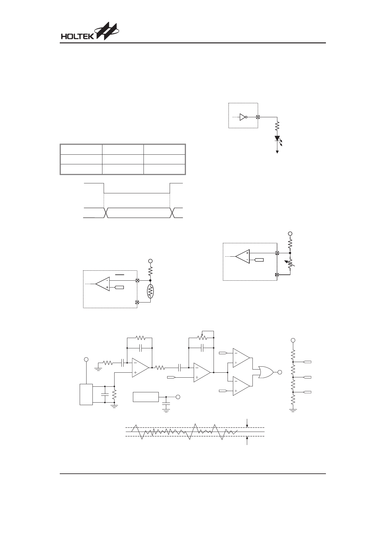
LED
The LED pin is a CMOS output pin which is used as a
valid trigger indicator. When the TRIAC/RELAY is acti-
vated, this pin will be active until the TRIAC/RELAY has
is switched OFF. The LED pin structure is shown in
Fig.9.
R E L A Y /L E D
1kW
T r ig g e r
In d ic a to r
Fig. 9 LED Pin Drive LED
LVD
LVD is a low voltage detector. When the detected volt-
age is lower than 1.1V, the LED flicker and the buzzer
will emit a tone.
In Fig10, assume RX, RLVD can be adjusted to obtain the
desired voltage detection level.
V DD
RX
B U Z /L V D
1 .1 V
R LV D
T E S T /S C
Fig.10 LVD Application Example
VREF
D
S
G
PIR
Sensor
Comparator
Input
OP1
Regulator
VM
OP2
VREF
VH
Comp1
VL Comp2
VH
VL
PIR Amplifier
VREF
VH
Output
VM
VL
Rev. 1.50
6
February 21, 2011
Share Link: 