IDT7132 查看數據表(PDF) - Integrated Device Technology
零件编号
产品描述 (功能)
比赛名单
IDT7132 Datasheet PDF : 16 Pages
| |||
IDT7132SA/LA and IDT 7142SA/LA
High Speed 2K x 8 Dual Port Static RAM
Military, Industrial and Commercial Temperature Ranges
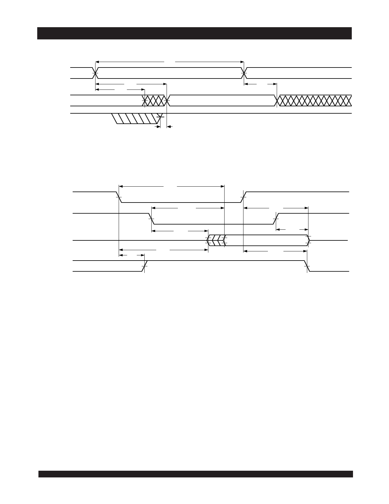
Timing Waveform of Read Cycle No. 1, Either Side(1)
ADDRESS
DATAOUT
BUSYOUT
tAA
tOH
PREVIOUS DATA VALID
tRC
tOH
DATA VALID
tBDDH(2,3)
2692 drw 07
Timing Waveform of Read Cycle No. 2, Either Side(1)
CE
OE
DATAOUT
ICC
CURRENT
ISS
tACE
tAOE(3)
tLZ(4)
tLZ(4)
tPU
50%
tHZ(5)
tHZ(5)
VALID DATA
tPD(3)
50%
2692 drw 08
NOTES:
1. R/W = VIH, CE = VIL, and is OE = VIL. Address is valid prior to the coincidental with CE transition LOW.
2. tBDD delay is required only in the case where the opposite port is completing a write operation to the same address location. For simultaneous read operations, BUSY has
no relationship to valid output data.
3. Start of valid data depends on which timing becomes effective last tAOE, tACE, tAA, and tBDD.
4. Timing depends on which signal is asserted last, OE or CE.
5. Timing depends on which signal is de-asserted first, OE or CE.
8
Share Link: 