IDT7132 查看數據表(PDF) - Integrated Device Technology
零件编号
产品描述 (功能)
比赛名单
IDT7132 Datasheet PDF : 16 Pages
| |||
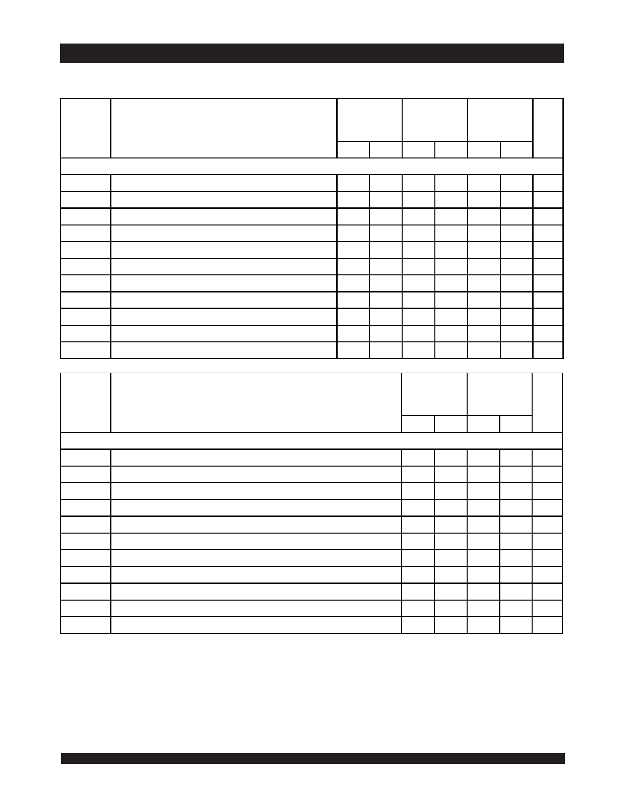
IDT7132SA/LA and IDT 7142SA/LA
High Speed 2K x 8 Dual Port Static RAM
Military, Industrial and Commercial Temperature Ranges
AC Electrical Characteristics Over the
Operating Temperature Supply Voltage Range(5,6)
7132X20(2)
7142X20(2)
Com'l Only
7132X25(2)
7142X25(2)
Com'l, Ind
& Military
7132X35
7142X35
Com'l &
Military
Symbol
Parameter
Min. Max. Min. Max. Min. Max. Unit
WRITE CYCLE
tWC
Write Cycle Time(3)
tEW
Chip Enable to End-of-Write
tAW
Address Valid to End-of-Write
tAS
Address Set-up Time
tWP
Write Pulse Width(4)
tWR
Write Recovery Time
tDW
Data Valid to End-of-Write
tHZ
Output High-Z Time(1)
tDH
Data Hold Time
tWZ
Write Enable to Output in High-Z(1)
tOW
Output Active from End-of-Write(1)
20
____
25
____
35
____
ns
15
____
20
____
30
____
ns
15
____
20
____
30
____
ns
0
____
0
____
0
____
ns
15
____
15
____
25
____
ns
0
____
0
____
0
____
ns
10
____
12
____
15
____
ns
____
10
____
10
____
15
ns
0
____
0
____
0
____
ns
____
10
____
10
____
15
ns
0
____
0
____
0
____
ns
2692 tbl 09
7132X55
7142X55
Com'l &
Military
7132X100
7142X100
Com'l &
Military
Symbol
Parameter
Min. Max. Min. Max. Unit
WRITE CYCLE
tWC
Write Cycle Time(3)
tEW
Chip Enable to End-of-Write
tAW
Address Valid to End-of-Write
tAS
Address Set-up Time
tWP
Write Pulse Width(4)
tWR
Write Recovery Time
tDW
Data Valid to End-of-Write
tHZ
Output High-Z Time(1)
55
____
100
____
ns
40
____
90
____
ns
40
____
90
____
ns
0
____
0
____
ns
30
____
55
____
ns
0
____
0
____
ns
20
____
40
____
ns
____
25
____
40
ns
tDH
Data Hold Time
0
____
0
____
ns
tWZ
Write Enable to Output in High-Z(1)
____
30
____
40
ns
tOW
Output Active from End-of-Write(1)
0
____
0
____
ns
NOTES:
2692 tbl 10
1. Transition is measured 0mV from Low or High-impedance voltage with Output Test Load (Figure 2). This parameter is guaranteed by device characterization
but is not production tested.
2. PLCC package only.
3. For Master/Slave combination, tWC = tBAA + tWP, since R/W = VIL must occur after tBAA.
4. If OE is LOW during a R/W controlled write cycle, the write pulse width must be the larger of tWP or (tWZ + tDW) to allow the I/O drivers to turn off data to be placed on the
bus for the required tDW. If OE is High during a R/W controlled write cycle, this requirement does not apply and the write pulse can be as short as the specified tWP.
5. 'X' in part numbers indicates power rating (SA or LA).
6. Industrial temperature: for specific speeds, packages and powers contact your sales office.
6.942
Share Link: 