81487EIB(2005) 查看數據表(PDF) - Intersil
零件编号
产品描述 (功能)
比赛名单
81487EIB Datasheet PDF : 14 Pages
| |||
ISL8487E, ISL81487L, ISL81487E
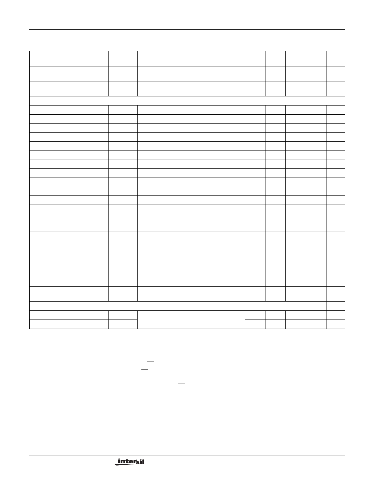
Electrical Specifications Test Conditions: VCC = 4.5V to 5.5V; Unless Otherwise Specified.
Typicals are at VCC = 5V, TA = 25°C, (Note 2) (Continued)
PARAMETER
SYMBOL
TEST CONDITIONS
TEMP
(°C) MIN
TYP MAX UNITS
Receiver Enable from Shutdown to tZH(SHDN) CL = 15pF, SW = GND, (Figure 5, Notes 7, 9)
Full
-
800 2500 ns
Output High
Receiver Enable from Shutdown to tZL(SHDN) CL = 15pF, SW = VCC, (Figure 5, Notes 7, 9)
Full
-
800 2500 ns
Output Low
SWITCHING CHARACTERISTICS (ISL81487L)
Driver Input to Output Delay
tPLH, tPHL RDIFF = 54Ω, CL = 100pF, (Figure 2)
Full
Driver Output Skew
tSKEW RDIFF = 54Ω, CL = 100pF, (Figure 2)
Full
Driver Differential Rise or Fall Time tR, tF RDIFF = 54Ω, CL = 100pF, (Figure 2)
Full
Driver Enable to Output High
tZH
CL = 100pF, SW = GND, (Figure 3, Note 5)
Full
Driver Enable to Output Low
tZL
CL = 100pF, SW = VCC, (Figure 3, Note 5)
Full
Driver Disable from Output High
tHZ
CL = 15pF, SW = GND, (Figure 3)
Full
Driver Disable from Output Low
tLZ
CL = 15pF, SW = VCC, (Figure 3)
Full
Receiver Input to Output Delay
tPLH, tPHL (Figure 4)
Full
Receiver Skew | tPLH - tPHL |
tSKD (Figure 4)
25
Receiver Enable to Output High
tZH
CL = 15pF, SW = GND, (Figure 5, Note 6)
Full
Receiver Enable to Output Low
tZL
CL = 15pF, SW = VCC, (Figure 5, Note 6)
Full
Receiver Disable from Output High
tHZ
CL = 15pF, SW = GND, (Figure 5)
Full
Receiver Disable from Output Low
tLZ
CL = 15pF, SW = VCC, (Figure 5)
Full
Maximum Data Rate
fMAX
Full
Time to Shutdown
tSHDN (Note 7)
Full
Driver Enable from Shutdown to tZH(SHDN) CL = 100pF, SW = GND, (Figure 3, Notes 7, 8) Full
Output High
150 650 1200 ns
-
160
600
ns
250 900 1200 ns
100 1000 1500 ns
100 1000 1500 ns
150 750 1500 ns
150 750 1500 ns
30
175 250
ns
-
13
-
ns
-
10
50
ns
-
10
50
ns
-
10
50
ns
-
10
50
ns
250
-
-
kbps
50
140 600
ns
-
1100 2000 ns
Driver Enable from Shutdown to
tZL(SHDN) CL = 100pF, SW = VCC, (Figure 3, Notes 7, 8)
Full
Output Low
-
1000 2000 ns
Receiver Enable from Shutdown to tZH(SHDN) CL = 15pF, SW = GND, (Figure 5, Notes 7, 9)
Full
-
900 2000 ns
Output High
Receiver Enable from Shutdown to tZL(SHDN) CL = 15pF, SW = VCC, (Figure 5, Notes 7, 9)
Full
-
900 2000 ns
Output Low
ESD PERFORMANCE
RS-485 Pins (A/Y, B/Z)
Human Body Model
25
-
±15
-
kV
All Other Pins
25
-
>±7
-
kV
NOTES:
2. Currents into device pins are positive; currents out of device pins are negative. Voltages are referenced to ground unless otherwise specified.
3. Supply current specification is valid for loaded drivers when DE = 0V.
4. Applies to peak current. See “Typical Performance Curves” for more information.
5. When testing the ISL8487E and ISL81487L, keep RE = 0 to prevent the device from entering SHDN.
6. When testing the ISL8487E and ISL81487L, the RE signal high time must be short enough (typically <200ns) to prevent the device from entering
SHDN.
7. The ISL8487E and ISL81487L are put into shutdown by bringing RE high and DE low. If the inputs are in this state for less than 50ns, the parts
are guaranteed not to enter shutdown. If the inputs are in this state for at least 600ns, the parts are guaranteed to have entered shutdown. See
“Low-Power Shutdown Mode” section.
8. Keep RE = VCC, and set the DE signal low time >600ns to ensure that the device enters SHDN.
9. Set the RE signal high time >600ns to ensure that the device enters SHDN.
10. Devices meeting these limits are denoted as “1/8 unit load (1/8 UL)” transceivers. The RS-485 standard allows up to 32 Unit Loads on the bus,
so there can be 256 1/8 UL devices on a bus.
6
FN6051.6
Share Link: 