LC86E5420 查看數據表(PDF) - SANYO -> Panasonic
零件编号
产品描述 (功能)
比赛名单
LC86E5420 Datasheet PDF : 21 Pages
| |||
LC86E5420
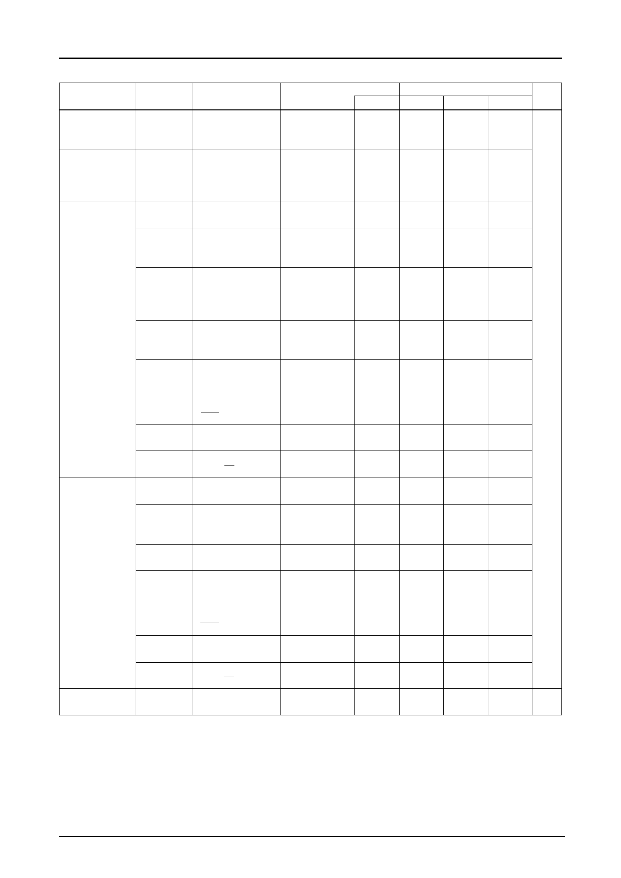
2. Recommended Operating Range at VSS=0V and Ta=+10°C to +40°C
Parameter
Symbol
Pins
Conditions VDD [V] min.
Ratings
typ.
Operating
VDD
VDD
0.98µs ≤ tCYC
4.5
supply
tCYC ≤ 400µs
voltage range
HOLD voltage VHD
VDD
RAMs and
2.0
Registers hold
voltage at HOLD
mode.
Input high
voltage
VIH(1)
Port 0 at CMOS Output disable 4.5 to 6.0 0.33VDD
output
+1.0
VIH(2)
Port 0 at N-ch
Output disable 4.0 to 6.0 0.75VDD
open drain output
option.
VIH(3)
•Port 1
•Ports 72, 73
Output disable 4.5 to 6.0 0.75VDD
•Port 3 at CMOS
output
VIH(4)
Port 3 at N-ch
Output disable 4.5 to 6.0 0.75VDD
open drain output
option.
VIH(5)
•Port 70
Port input /
Output disable 4.5 to 6.0 0.75VDD
interrupt
•Port 71
•RES
VIH(6)
Port 70
Output disable 4.5 to 6.0 0.9VDD
Watchdog timer
VIH(7)
•Port 8
•Ports 74, 75
Output disable 4.5 to 6.0 0.75VDD
Using as port
Input low
voltage
VIL(1)
Port 0 at CMOS Output disable 4.5 to 6.0 VSS
output option
VIL(2)
Port 0 at N-ch
Output disable 4.5 to 6.0 VSS
open drain output
option.
VIL(3)
•Ports 1, 3
•Ports 72, 73
Output disable 4.5 to 6.0 VSS
VIL(4)
•Port 70
Port input /
Output disable 4.5 to 6.0 VSS
interrupt
•Port 71
•RES
VIL(5)
Port 70
Output disable 4.5 to 6.0 VSS
Watchdog timer
VIL(6)
•Port 8
•Ports 74, 75
Output disable 4.5 to 6.0 VSS
Using as port
Operation
tCYC
4.5 to 6.0 0.98
cycle time
max. unit
6.0 V
6.0
VDD
13.5
VDD
13.5
VDD
VDD
VDD
0.2VDD
0.25VDD
0.25VDD
0.25VDD
0.8VDD
-- 1.0
0.25VDD
400 µs
No.6805-11/21
Share Link: 