LC86E5420 查看數據表(PDF) - SANYO -> Panasonic
零件编号
产品描述 (功能)
比赛名单
LC86E5420 Datasheet PDF : 21 Pages
| |||
LC86E5420
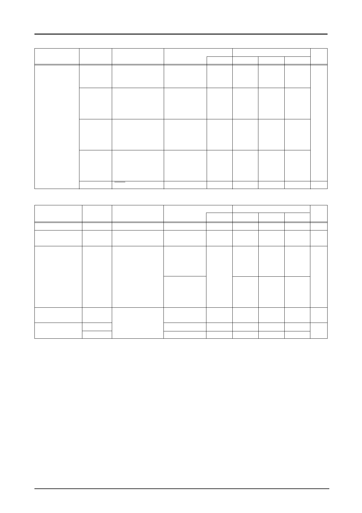
5. Pulse Input Conditions at VSS=0V and Ta=+10°C to +40°C
Ratings
Parameter
Symbol
Pins
Conditions VDD [V] min.
typ.
max. unit
High / low
tPIH(1) •INT0, INT1
•Interrupt accept- 4.5 to 6.0 1
tCYC
level pulse
tPIL(1) •INT2 / T0IN
able
width
•Timer0-countable
tPIH(2) INT3 / T0IN
•Interrupt accept- 4.5 to 6.0 2
tPIL(2) (The noise
able
rejection clock •Timer0-countable
select to 1 / 1.)
tPIH(3) INT3 / T0IN
•Interrupt accept- 4.5 to 6.0 32
tPIL(3) (The noise
able
rejection clock •Timer0-countable
select to 1 / 16.)
tPIL(4) INT3 / T0IN
•Interrupt accept- 4.5 to 6.0 128
tPIL(4) (The noise
able
rejection clock •Timer0-countable
select to 1 / 64.)
tPIL(5) RES
Reset acceptable 4.5 to 6.0 200
µs
6. A / D Converter Characteristics at VSS=0V and Ta=+10°C to +40°C
Ratings
Parameter
Symbol
Pins
Conditions VDD [V] min.
typ.
max. unit
Resolution
N
4.5 to 6.0
8
bit
Absolute
ET
precision (Note 2)
Conversion
tCAD
time
4.5 to 6.0
AD conversion 4.5 to 6.0 15.68
time=16 ! tCYC
(tCYC=
±1.5 LSB
65.28 µs
(tCYC=
(ADCR2=0)
0.98µs)
4.08µs)
(Note 3)
AD conversion
time=32 ! tCYC
31.36
(tCYC=
130.56
(tCYC=
(ADCR2=1)
0.98µs)
4.08µs)
(Note 3)
Analog input
voltage range
VAIN AN0 to AN7
4.5 to 6.0 VSS
VDD V
Analog port
IAINH
VAIN=VDD 4.5 to 6.0
input current
IAINL
VAIN=VSS 4.5 to 6.0 --1
(Note 2) Absolute precision excepts quantizing error (±1 / 2 LSB).
1
µA
(Note 3) The conversion time means the time from executing the AD conversion instruction to setting the complete
digital conversion value to the register.
No.6805-15/21
Share Link: 