LC863416C 查看數據表(PDF) - SANYO -> Panasonic
零件编号
产品描述 (功能)
比赛名单
LC863416C Datasheet PDF : 18 Pages
| |||
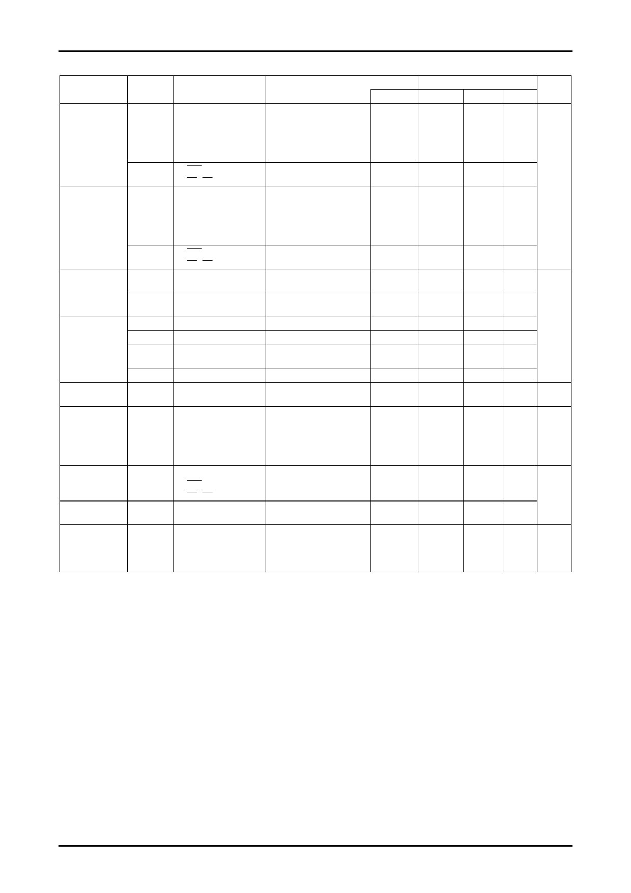
LC863448C/40C/32C/28C/24C/20C/16C
Electrical Characteristics at Ta = -10°C to +70°C, VSS = 0V
Parameter
High level input
current
Symbol
IIH(1)
Low level input
current
IIH(2)
IIL(1)
IIL(2)
High level
output voltage
VOH(1)
VOH(2)
Low level output
voltage
VOL(1)
VOL(2)
VOL(3)
Pull-up MOS
Tr. resistance
Bus terminal
short circuit
resistance
(SCL0-SCL1,
SDA0-SDA1)
Hysteresis
voltage
VOL(4)
Rpu
RBS
VHYS
Input clump
voltage
Pin capacitance
VCLMP
CP
Pins
Ports 0, 1, 3, 7
• RES
• HS , VS
Ports 0, 1, 3, 7
• RES
• HS , VS
• CMOS output of
ports 0, 1, 3, 71 to 73
R, G, B, BL
Ports 0, 1, 3, 71 to 73
Ports 0, 3, 71 to 73
• R, G, B, BL
• Port 1
Port 70
Ports 0, 1, 3, 7
• P10 to P12
• P11 to P13
• Ports 1, 3, 7
• RES
• HS , VS
CVIN
All pins
Conditions
•Output disable
•Pull-up MOS Tr. OFF
•VIN=VDD
(including the off-leak
current of the output Tr.)
•VIN=VDD
•Output disable
•Pull-up MOS Tr. OFF
•VIN=VSS
(including the off-leak
current of the output Tr.)
VIN=VSS
IOH=-1.0mA
IOH=-0.1mA
R. G. B: digital mode
IOL=10mA
IOL=1.6mA
IOL=3.0mA
R. G. B: digital mode
IOL=1mA
VOH=0.9VDD
Output disable
• f=1MHz
• Every other terminals are
connected to VSS.
• Ta=25ºC
VDD[V]
4.5 to 5.5
4.5 to 5.5
4.5 to 5.5
4.5 to 5.5
4.5 to 5.5
4.5 to 5.5
4.5 to 5.5
4.5 to 5.5
4.5 to 5.5
4.5 to 5.5
4.5 to 5.5
4.5 to 5.5
4.5 to 5.5
5.0
4.5 to 5.5
Ratings
min
typ
unit
max
1
1
μA
-1
-1
VDD-1
VDD-0.5
13
1.5
V
0.4
0.4
0.4
38
80 kΩ
130
300
Ω
0.1VDD
2.3
2.5
V
2.7
10
pF
No.A0117-11/18
Share Link: 