M37640E8FP 查看數據表(PDF) - Mitsumi
零件编号
产品描述 (功能)
比赛名单
M37640E8FP Datasheet PDF : 96 Pages
| |||
Ver 1.4
MITSUBISHI MICROCOMPUTERS
7640 Group
SINGLE-CHIP 8-BIT CMOS MICROCOMPUTER
1.12.5 Hold Function
1.12.6 Expanded Data Memory Access
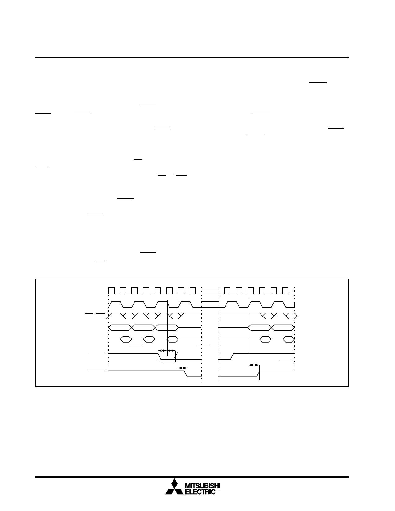
The hold function is used when the MCU is put in a
system where more than one device will need control
of the external address and data buses. Two signals
are used to implement this function, HOLD (P71) and
HLDA (P73). HOLD is an input to the MCU and is
brought low when an external device wants the MCU
to relinquish the address and data buses. HLDA is an
output from the MCU that signals when the MCU has
relinquished the buses. When this is the case, the
MCU tri-state ports 0 and 1 (address bus) and port 2
(data bus), and holds port P37 (RD) and port P36
(WR) high. Ports P37 and P36 are held high to pre-
vent any external device that is enabled by RD or WR
from being falsely activated. The clocks to the CPU
are stopped, but the peripheral clocks and port P34
(Fout) continue to oscillate. HOLD is brought high to
allow the MCU to regain the address and data buses.
When this occurs, HLDA will go high and ports P1, P2,
P37 and P36 will begin to drive the external buses
again. The timing for the hold function is shown in Fig-
ure 1.12. The hold function is only valid for memory
expansion and microprocessor modes. Bit 5 of CPMB
is used to enable the hold function. HLDA will loose
its function when the IBF1 pin functionality is used.
The Expanded Data Memory Access (EDMA) mode
feature allows the user to access a greater than 64
Kbyte data area for instructions LDA (IndY) with T=“0”
and T=“1”, and STA (IndY). Bit 4 of CPMB is used to
enable/disable the EDMA function. If bit 4 of CPMB
equals “1”, then during the data read/write cycle of in-
structions LDA (IndY) and STA (IndY) Port 40 (EDMA)
is driven low. The EDMA signal output can be used by
an external decoder to indicate when the read/write is
to a different 64 Kbyte bank. The actual determination
of which bank to access can be done by using a few
bits of a port to represent the extended addresses
above AB15. For example, if four banks are accessed,
then two bits are needed to uniquely identify each
bank. Two port bits can be used for this, one repre-
senting AB16 and the other AB17. The instruction
sequences for STA (IndY) and LDA (IndY) are shown in
Figure 1.13 and Figure 1.14.
XIN
Φout
RD, WR
ADDRout
DATAin/out
HOLD
HLDA
////////
////////
------
------
------
tsu(HOLD-Φout)
th(Φout-HOLD)
td(Φout-HLDA)
------
------
Fig. 1.12. Hold Function Timing Diagram
td(Φout-HLDA)
14
Share Link: 