M37640E8FP 查看數據表(PDF) - Mitsumi
零件编号
产品描述 (功能)
比赛名单
M37640E8FP Datasheet PDF : 96 Pages
| |||
Ver 1.4
MITSUBISHI MICROCOMPUTERS
7640 Group
SINGLE-CHIP 8-BIT CMOS MICROCOMPUTER
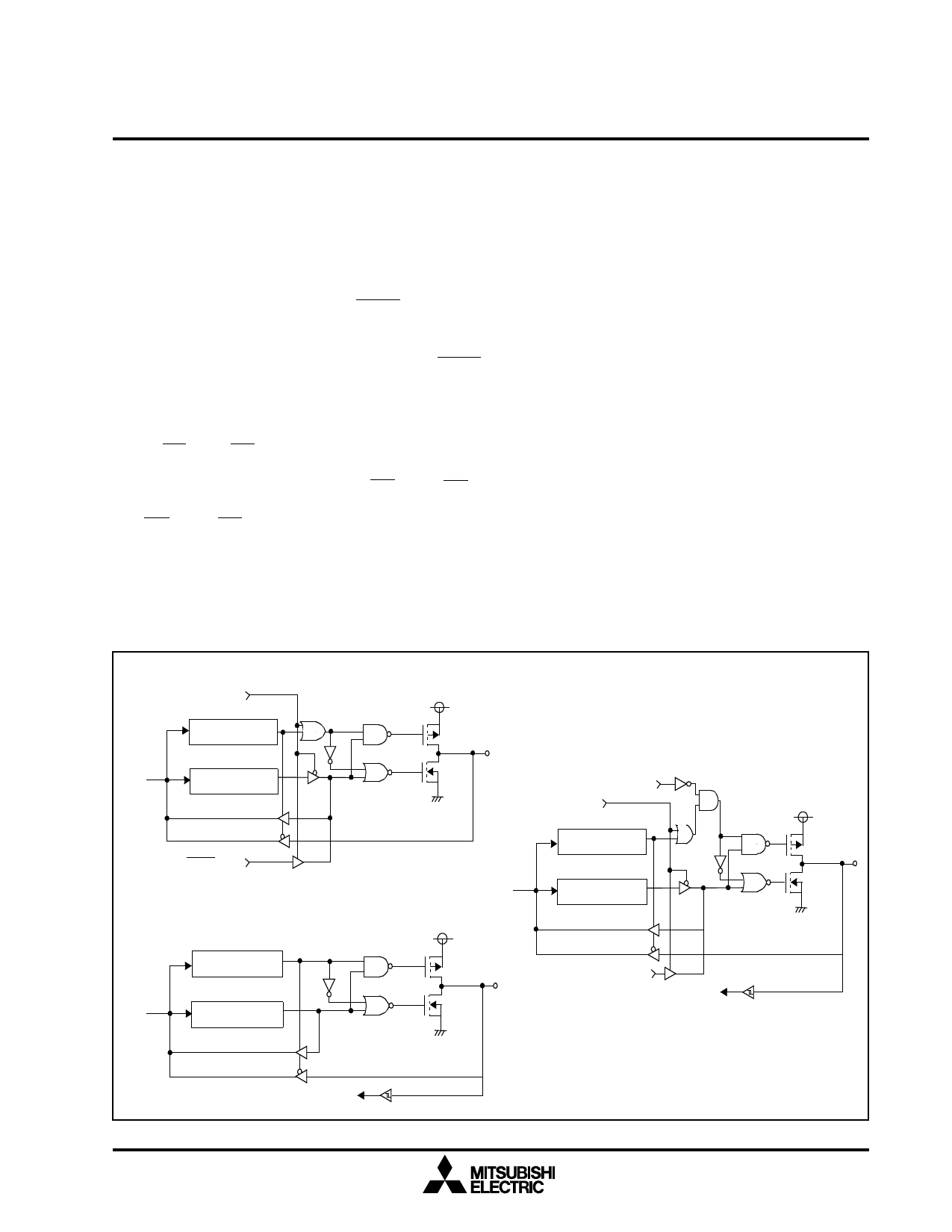
1.14.1.3 Port P4
Port 4 is a 5-bit general purpose I/O port that can be
configured to access special second functions. The
port can be set up in any configuration in all three pro-
cessor modes.
Port P40
This pin is multiplexed with the EDMA (Extended
Data Memory Access) function. When the MCU is in
memory expansion or microprocessor mode and
CPMB4 is set to “1”, this pin operates as the EDMA
output as described in section 1.12.6.
Port P41- P42
These pins are multiplexed with external interrupts 0
and 1 (INT0 and INT1). The external interrupt function
is enabled by setting the bits to “1” in the interrupt
control register that correspond to INT0 and INT1.
The interrupt polarity register can be configured to de-
fine INT0 and INT1 as active high or low interrupts.
See section 1.15.1 for more information on configur-
ing interrupts.
Port P43- P44
These pins are multiplexed with Timer X and Y func-
tions for P43 and P44 respectively. The timer
functions of the pins are independently defined by
configuring the timer peripheral. P43 acts as Timer X
input pin for pulse width measurement mode and
event counter mode or as Timer X output pin for pulse
output mode. P43 can also be used as an external in-
terrupt (CNTR0) when Timer X in not in output mode.
The polarity is selected in the Timer X mode register.
The external interrupt function is enabled by setting
the bit to “1” in the interrupt control register that corre-
sponds to CNTR0. See section 1.15.1 for more
information on configuring interrupts.
P44 acts as Timer Y input pin for pulse period mea-
surement mode, pulse H-L measurement mode, and
event counter mode or as Timer Y output pin for pulse
output mode. P43 can also be used as an external in-
terrupt (CNTR1) when Timer Y in not in output mode.
The polarity is selected in the Timer Y mode register.
The external interrupt function is enabled by setting
the bit to “1” in the interrupt control register that corre-
sponds to CNTR1. See section 1.15.1 for more
information on configuring interrupts.
Port P40
CPMB4
Direction Register
Data Bus
Port Latch
EDMA Signal
Port P41 and P42
Direction Register
Data Bus
Port Latch
Port P43 and P44
Timer Counter Input Enable
Pulse Output Mode Enable
Direction Register
Data Bus
Port Latch
Timer X, Y Output
CNTR0, 1 Input
Interrupt Input
Fig. 1.16. Port P4 Block Diagram
19
Share Link: 