LC75878W 查看數據表(PDF) - SANYO -> Panasonic
零件编号
产品描述 (功能)
比赛名单
LC75878W Datasheet PDF : 33 Pages
| |||
LC75878E, 75878W
Control Data Functions
1. PC1 to PC4: General-purpose output port state setting data
These control data bits set the states of the general-purpose output ports P1 to P4.
Output pin
P1
P2
P3
P4
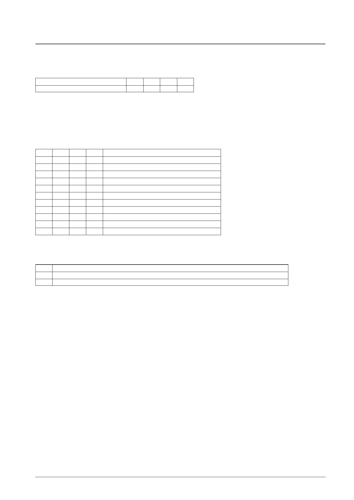
General-purpose output port state setting data PC1 PC2 PC3 PC4
For example, if PC1 and PC2 are set to 1, and PC3 and PC4 are set to 0, then the output pins P1 and P2 will output high
levels (VDD) and the output pins P3 and P4 will output low levels (VSS).
2. CT0 to CT3, CTC: Display contrast setting data
These control data bits set the display contrast.
CT0 to CT3: Display contrast setting (11 steps)
CT0
0
1
0
1
0
1
0
1
0
1
0
CT1
0
0
1
1
0
0
1
1
0
0
1
CT2
0
0
0
0
1
1
1
1
0
0
0
CT3
0
0
0
0
0
0
0
0
1
1
1
LCD drive 4/4 bias voltage supply VLCD0 level
0.94 VLCD = VLCD – (0.03 VLCD × 2)
0.91 VLCD = VLCD – (0.03 VLCD × 3)
0.88 VLCD = VLCD – (0.03 VLCD × 4)
0.85 VLCD = VLCD – (0.03 VLCD × 5)
0.82 VLCD = VLCD – (0.03 VLCD × 6)
0.79 VLCD = VLCD – (0.03 VLCD × 7)
0.76 VLCD = VLCD – (0.03 VLCD × 8)
0.73 VLCD = VLCD – (0.03 VLCD × 9)
0.70 VLCD = VLCD – (0.03 VLCD × 10)
0.67 VLCD = VLCD – (0.03 VLCD × 11)
0.64 VLCD = VLCD – (0.03 VLCD × 12)
CTC: Display contrast adjustment circuit state setting
CTC
0
1
Display contrast adjustment circuit state
The display contrast adjustment circuit is disabled, and the VLCD0 pin level is forced to the VLCD level.
The display contrast adjustment circuit operates and the display contrast is adjusted.
Note that although the display contrast can be adjusted by operating the built-in display contrast adjustment circuit, it is
also possible to apply fine adjustments to the contrast by connecting an external variable resistor to the VLCD4 pin and
modifying the VLCD4 pin voltage. However, the following conditions must be met: (VLCD0 – VLCD4) ≥ 4.5 V, and 1.5 V
≥ VLCD4 ≥ 0 V.
No. 6473-14/33
Share Link: 