LC75878W 查看數據表(PDF) - SANYO -> Panasonic
零件编号
产品描述 (功能)
比赛名单
LC75878W Datasheet PDF : 33 Pages
| |||
LC75878E, 75878W
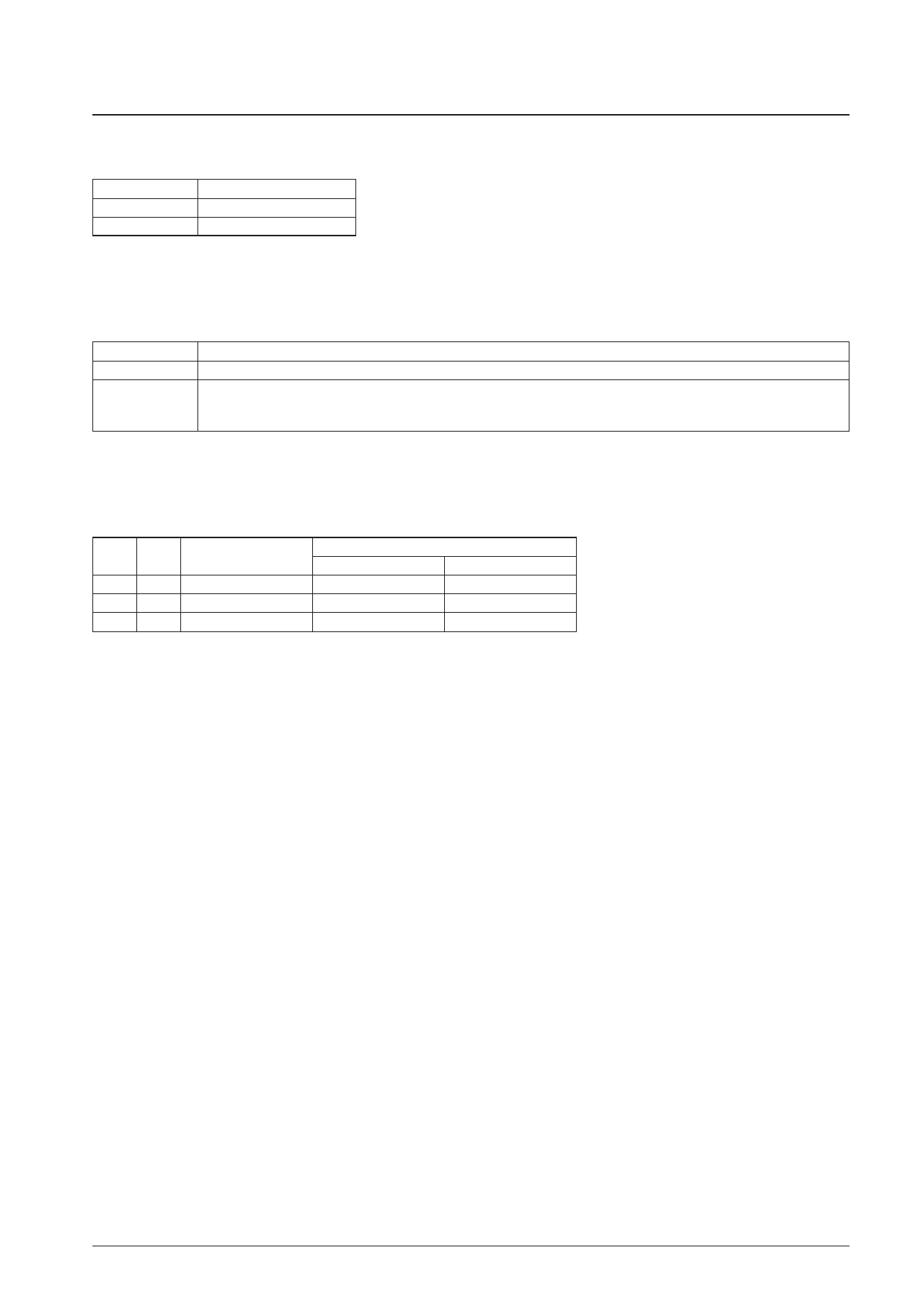
3. SC: Segment on/off control data
This control data bit controls the on/off state of the segments.
SC
Display state
0
On
1
Off
However, note that when the segments are turned off by setting SC to 1, the segments are turned off by outputting segment off waveforms from the segment
output pins.
4. BU: Normal mode/power saving mode control data
This control data bit controls the normal mode and power saving mode.
BU
Mode
0
Normal mode
Power saving mode
1
The common and segment pins go to the VLCD4 level and the oscillator on the OSC pin is stopped. Note that the states of the
general-purpose output ports P1 to P4 are set by PC1 to PC4 in the control data during power saving mode as well as normal mode.
5. DT1, DT2: Display technique setting data
This control data bits set the display technique.
DT1 DT2
Display technique
0
0
1/8 duty 1/4 bias drive
1
0
1/9 duty 1/4 bias drive
0
1
1/10 duty 1/4 bias drive
Notes: Sn (n = 74 or 75): Segment outputs
COMn (n = 9 or 10): Common outputs
Output pins
S75/COM9
S74/COM10
S75
S74
COM9
S74
COM9
COM10
No. 6473-15/33
Share Link: 