MAX6006 查看數據表(PDF) - Maxim Integrated
零件编号
产品描述 (功能)
比赛名单
MAX6006 Datasheet PDF : 8 Pages
| |||
MAX6006–MAX6009
1µA SOT23 Precision Shunt
Voltage Reference
Pin Description
PIN
SOT23
SO
1
6, 8
2
4
3
—
—
1, 2, 3, 5, 7
NAME
OUT
GND
IC
N.C.
FUNCTION
Output Voltage. Bias OUT with a pullup resistor to a potential greater than OUT. Bypass
OUT to GND with a 0.01µF or larger capacitor.
Ground
Internally connected test point. Leave this pin unconnected, or connect to GND.
No connection. Not internally connected.
Detailed Description
The MAX6006–MAX6009 are precision, two-terminal,
series bandgap voltage references. On-chip thin-film
resistors are laser trimmed to provide 0.2% output volt-
age accuracies. Voltages of +1.25V, +2.048V, +2.5V, and
+3.0V are available in the space-saving SOT23 package
(2.1mm 5 2.7mm).
Applications Information
Output/Load Capacitance
For devices in this family, OUT needs to be bypassed to
GND with a 0.01µF or larger capacitor. In applications
where the load or the supply can experience step changes,
additional capacitance will reduce the amount of overshoot
(or undershoot) and assist the circuit’s transient response.
Output Voltage Hysteresis
Output voltage hysteresis is the change in the output volt-
age at TA = +25°C before and after the device is cycled
over its entire operating temperature range. Hysteresis is
caused by differential package stress appearing across
the bandgap core transistors. The temperature hysteresis
value is typically less than 200ppm.
Turn-On Time
The output capacitance and bias current of the MAX6006–
MAX6009 greatly affects turn-on settling time. In the
Typical Operating Characteristics, turn-on time is shown
with a 10nF output capacitor and a 1.2µA bias current.
Under these conditions, the MAX6006–MAX6009 settle
in 40ms. Settling time will linearly decrease in proportion
to the circuit’s bias current.
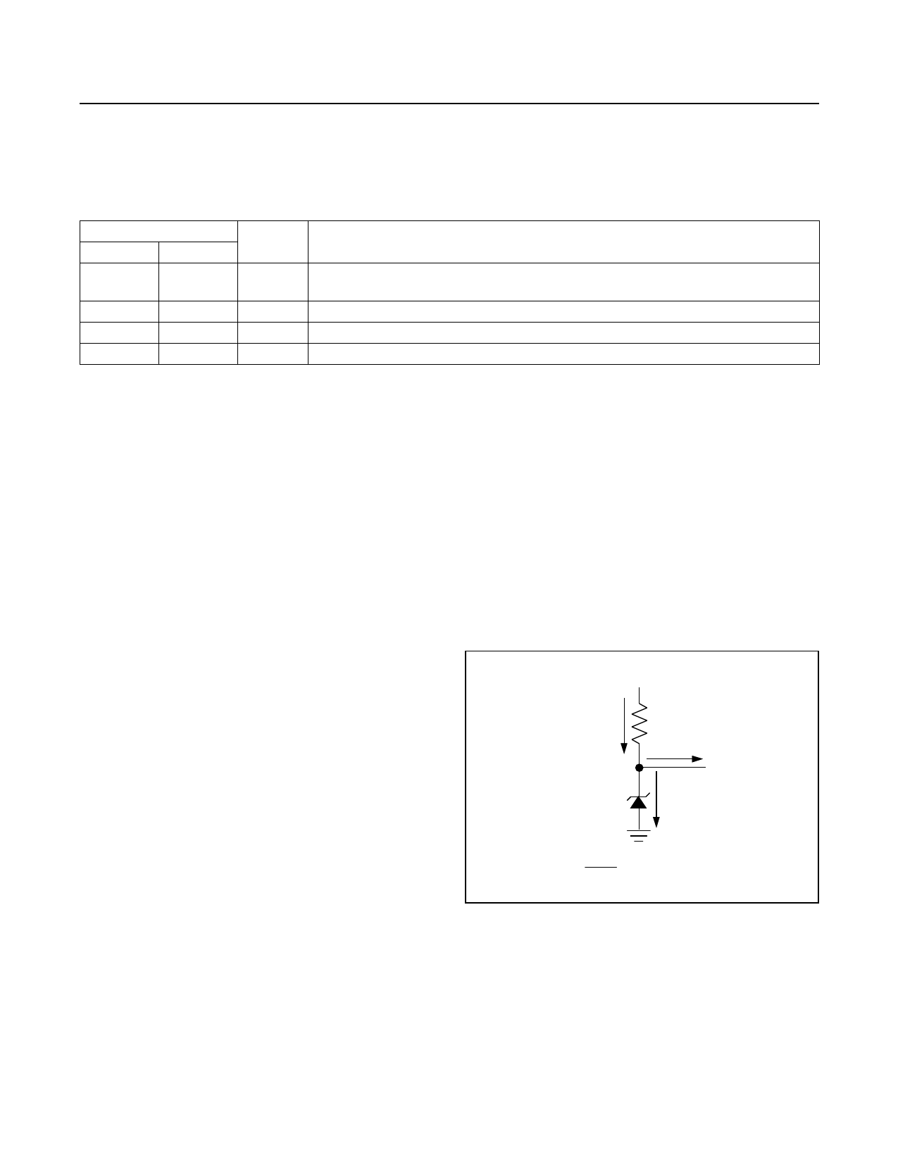
Typical Applications
In the typical shunt regulator application shown in
Figure 1, RBIAS is used to set the current through the
load (IL) and the current through the shunt regulator
(IRMIN). There are two worst-case situations that RBIAS
needs to be sized for:
1) RBIAS must be small enough that when VS (supply
voltage) is at its minimum and IL is at its maximum,
IRMIN is equal to at least the minimum operating
current of the shunt regulator.
2) RBIAS must be large enough that when VS is at its
maximum and IL is at its minimum, IRMIN is < 2mA.
VS
IRMIN + IL
VR
MAX6006
MAX6007
MAX6008
MAX6009
RBIAS
= VS
IL +
- VR
IRMIN
RBIAS
IL
IRMIN
VOUT
Figure 1. Typical Application Circuit
www.maximintegrated.com
Maxim Integrated │ 6
Share Link: 