MAX7432AEUD 查看數據表(PDF) - Maxim Integrated
零件编号
产品描述 (功能)
比赛名单
MAX7432AEUD Datasheet PDF : 21 Pages
| |||
Standard Definition Video Reconstruction
Filters and Buffers
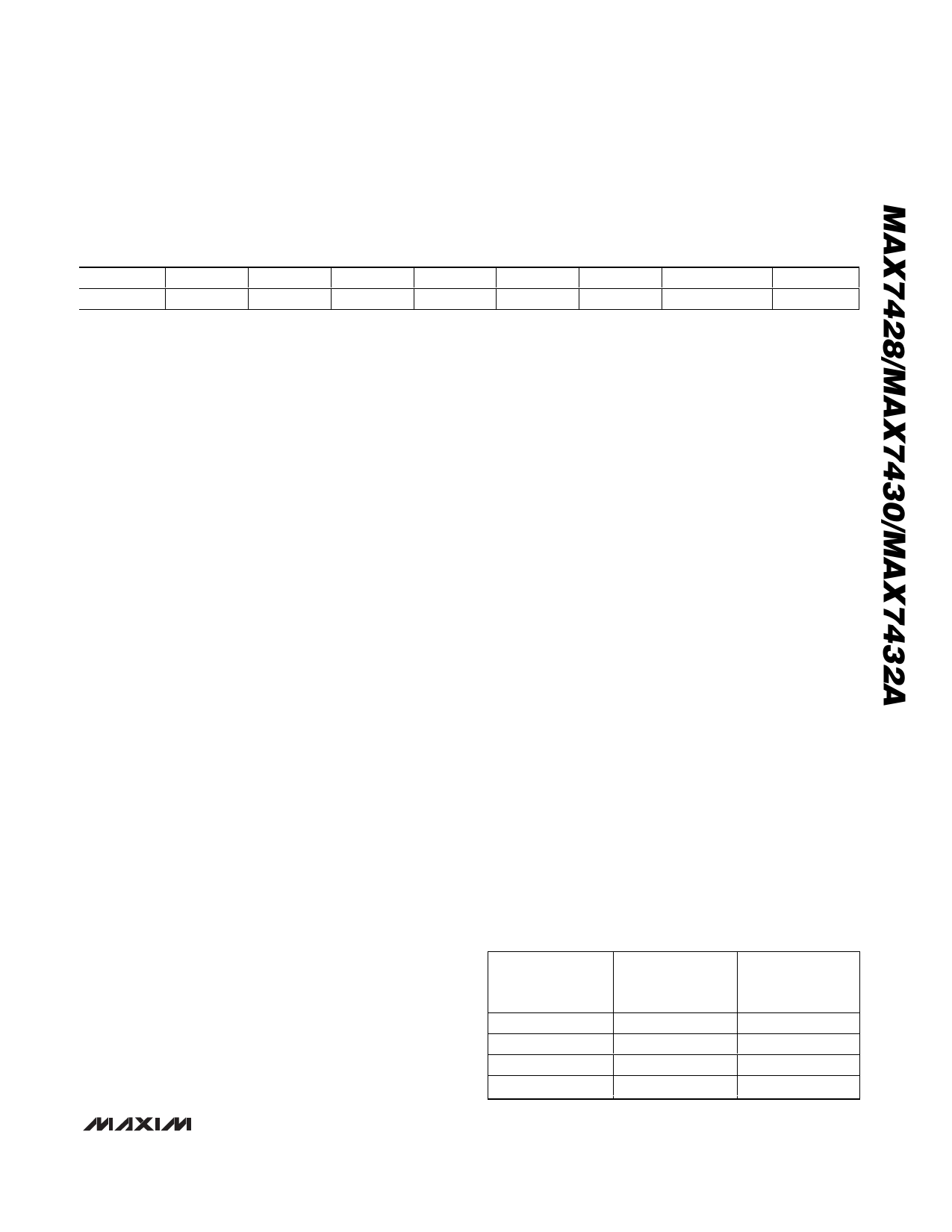
Table 1. MAX7428 Control Register
NAME
DEFAULT
(MSB)
SYNCIO
0
ABSEL
1
BYPASS
1
CLEVEL
0
BOOST1
0
BOOST0
0
OUTDISABLE
0
FIRST BIT
(LSB)
—
0
Filter
Filter Response
The reconstruction filter consists of a 6th-order
Butterworth filter in three second-order stages. The
Butterworth filter features a maximally flat passband for
NTSC and PAL bandwidths. The stopband offers typical-
ly 50dB of attenuation at sampling frequencies of 25MHz
and above (see Typical Operating Characteristics).
The corner frequency is not critical since the response
of the filter meets both the stopband and passband
specifications. The MAX7428/MAX7430/MAX7432A
incorporate an autotrimming feature that reduces the
corner frequency variation digitally. It is possible,
although not likely, that a discrete shift in the corner fre-
quency may occur due to an external environmental
change. The autotrimming operates continuously so
that the corner frequency remains centered over the full
operating temperature range.
High-Frequency Boost
The high-frequency boost compensates for signal degra-
dation and roll-off in the signal path prior to the MAX7428/
MAX7430/MAX7432A. High-frequency boost is program-
mable in four steps to increase image sharpness.
Output Buffer
The output buffer is able to drive two 150Ω video loads
with a 2Vp-p signal. The +6dB gain of the output buffer
is independent of the filter bypass or input selection.
The output buffer drives the 75Ω backmatch resistors
and series capacitor (typically 220µF). The MAX7428/
MAX7430/MAX7432A are able to drive the video load
directly without using the 220µF capacitor. This feature
is common in SCART applications. The OUTDISABLE bit
of the control register disables the output (mute) (see
Control Register section).
Filter Bypass
The MAX7428/MAX7430/MAX7432A offer selectable fil-
ter bypassing that allows either of the video inputs to
be filtered or unfiltered. The 1MΩ optional input resis-
tors are needed only in filter bypass mode to provide a
discharge path for the input coupling capacitors.
Serial Interface
Maxim’s Single Pin Bus (MSPB) interface uses DATA to
transfer data to and from the microprocessor (µP) and
the MAX7428/MAX7430/MAX7432A. This negative logic
protocol uses three different pulse widths to represent
a logic “1”, logic “0”, and control commands. MSPB
allows up to 16 devices to be connected on the same
bus by assigning a unique 4-bit identification address
to each device. The µP can communicate to each
device individually or by sending a “broadcast” mes-
sage to all the devices. The unique address for each
device is set by means of the time constant set by the
external capacitor connected in parallel with the exter-
nal 300kΩ resistor (see Initializing the MAX7428/
MAX7430/MAX7432A section).
MAX7428 Control Register
Table 1 defines the structure of the MAX7428 8-bit con-
trol register programmed by MSPB. This register con-
trols the selection of INA or INB, SYNCIO functionality,
filter bypassing, clamp-level selection, high-frequency
boost control, and output disable. See Maxim’s Single
Pin Bus Interface (MSPB) section for detailed program-
ming instructions.
SYNCIO: SYNCIO Select bit. A logic 0 sets the SYNCIO
pin to function as an output while a logic 1 sets SYNCIO
to function as an input.
ABSEL: Channel Select bit. A logic 0 selects the input
at INB to be processed while a logic 1 selects the input
at INA to be processed.
BYPASS: Filter Bypass Select bit. A logic 1 selects the
filter while a logic 0 bypasses the filter.
Table 2. Boost Level Programming
BOOST1
0
0
1
1
BOOST0
0
1
0
1
RELATIVE HIGH
FREQUENCY
BOOST
0
0.3db to 0.5db
0.6db to 1.0db
0.9db to 1.5db
_______________________________________________________________________________________ 9
Share Link: 