MC14012B(2011) 查看數據表(PDF) - ON Semiconductor
零件编号
产品描述 (功能)
比赛名单
MC14012B Datasheet PDF : 8 Pages
| |||
MC14012B
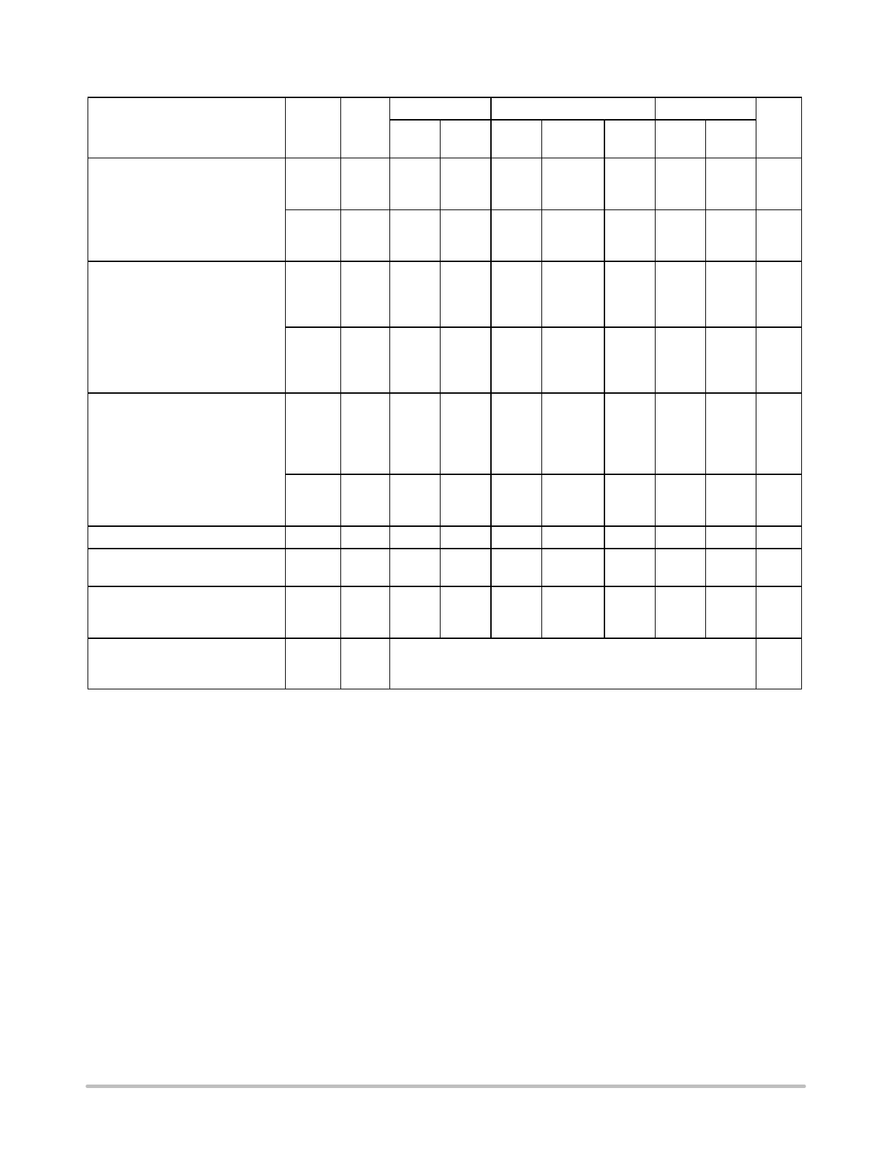
ÎÎÎÎÎÎÎÎÎÎÎÎÎÎÎÎÎÎÎÎÎÎÎÎÎÎÎÎÎÎÎÎÎ ELECTRICAL CHARACTERISTICS (Voltages Referenced to VSS)
ÎÎÎÎÎÎÎÎÎÎÎÎÎÎÎÎÎÎÎÎÎÎÎÎÎÎÎÎÎÎÎÎÎÎÎÎÎÎÎÎÎÎÎÎÎÎÎÎÎÎÎÎÎÎÎÎÎÎÎÎÎÎÎÎÎÎ Characteristic
Symbol
VDD
Vdc
− 55_C
Min Max
ÎÎÎÎÎÎÎÎÎÎÎÎÎÎÎÎÎÎÎÎÎÎÎÎÎÎÎÎÎÎÎÎÎ Output Voltage
ÎÎÎÎÎÎÎÎÎÎÎÎÎÎÎÎÎÎÎÎÎÎÎÎÎÎÎÎÎÎÎÎÎ Vin = VDD or 0
“0” Level VOL
ÎÎÎÎÎÎÎÎÎÎÎÎÎÎÎÎÎÎÎÎÎÎÎÎÎÎÎÎÎÎÎÎÎÎÎÎÎÎÎÎÎÎÎÎÎÎÎÎÎÎÎÎÎÎÎÎÎÎÎÎÎÎÎÎÎÎ Vin = 0 or VDD
“1” Level VOH
ÎÎÎÎÎÎÎÎÎÎÎÎÎÎÎÎÎÎÎÎÎÎÎÎÎÎÎÎÎÎÎÎÎÎÎÎÎÎÎÎÎÎÎÎÎÎÎÎÎÎÎÎÎÎÎÎÎÎÎÎÎÎÎÎÎÎ Input Voltage
“0” Level VIL
ÎÎÎÎÎÎÎÎÎÎÎÎÎÎÎÎÎÎÎÎÎÎÎÎÎÎÎÎÎÎÎÎÎ (VO = 4.5 or 0.5 Vdc)
(VO = 9.0 or 1.0 Vdc)
ÎÎÎÎÎÎÎÎÎÎÎÎÎÎÎÎÎÎÎÎÎÎÎÎÎÎÎÎÎÎÎÎÎ (VO = 13.5 or 1.5 Vdc)
ÎÎÎÎÎÎÎÎÎÎÎÎÎÎÎÎÎÎÎÎÎÎÎÎÎÎÎÎÎÎÎÎÎ “1”Level VIH
ÎÎÎÎÎÎÎÎÎÎÎÎÎÎÎÎÎÎÎÎÎÎÎÎÎÎÎÎÎÎÎÎÎ (VO = 0.5 or 4.5 Vdc)
(VO = 1.0 or 9.0 Vdc)
ÎÎÎÎÎÎÎÎÎÎÎÎÎÎÎÎÎÎÎÎÎÎÎÎÎÎÎÎÎÎÎÎÎ (VO = 1.5 or 13.5 Vdc)
ÎÎÎÎÎÎÎÎÎÎÎÎÎÎÎÎÎÎÎÎÎÎÎÎÎÎÎÎÎÎÎÎÎ Output Drive Current
ÎÎÎÎÎÎÎÎÎÎÎÎÎÎÎÎÎÎÎÎÎÎÎÎÎÎÎÎÎÎÎÎÎ (VOH = 2.5 Vdc)
(VOH = 4.6 Vdc)
ÎÎÎÎÎÎÎÎÎÎÎÎÎÎÎÎÎÎÎÎÎÎÎÎÎÎÎÎÎÎÎÎÎ (VOH = 9.5 Vdc)
(VOH = 13.5 Vdc)
IOH
Source
ÎÎÎÎÎÎÎÎÎÎÎÎÎÎÎÎÎÎÎÎÎÎÎÎÎÎÎÎÎÎÎÎÎÎÎÎÎÎÎÎÎÎÎÎÎÎÎÎÎÎÎÎÎÎÎÎÎÎÎÎÎÎÎÎÎÎ (VOL = 0.4 Vdc)
(VOL = 0.5 Vdc)
ÎÎÎÎÎÎÎÎÎÎÎÎÎÎÎÎÎÎÎÎÎÎÎÎÎÎÎÎÎÎÎÎÎ (VOL = 1.5 Vdc)
Sink IOL
ÎÎÎÎÎÎÎÎÎÎÎÎÎÎÎÎÎÎÎÎÎÎÎÎÎÎÎÎÎÎÎÎÎ Input Current
Iin
ÎÎÎÎÎÎÎÎÎÎÎÎÎÎÎÎÎÎÎÎÎÎÎÎÎÎÎÎÎÎÎÎÎ Input Capacitance
Cin
(Vin = 0)
ÎÎÎÎÎÎÎÎÎÎÎÎÎÎÎÎÎÎÎÎÎÎÎÎÎÎÎÎÎÎÎÎÎÎÎÎÎÎÎÎÎÎÎÎÎÎÎÎÎÎÎÎÎÎÎÎÎÎÎÎÎÎÎÎÎÎ Quiescent Current
IDD
(Per Package)
ÎÎÎÎÎÎÎÎÎÎÎÎÎÎÎÎÎÎÎÎÎÎÎÎÎÎÎÎÎÎÎÎÎÎÎÎÎÎÎÎÎÎÎÎÎÎÎÎÎÎÎÎÎÎÎÎÎÎÎÎÎÎÎÎÎÎ Total Supply Current (Notes 3, 4)
IT
(Dynamic plus Quiescent,
ÎÎÎÎÎÎÎÎÎÎÎÎÎÎÎÎÎÎÎÎÎÎÎÎÎÎÎÎÎÎÎÎÎÎÎÎÎÎÎÎÎÎÎÎÎÎÎÎÎÎÎÎÎÎÎÎÎÎÎÎÎÎÎÎÎÎ Per Gate, CL = 50 pF)
5.0
−
0.05
10
−
0.05
15
−
0.05
5.0
4.95
−
10
9.95
−
15 14.95
−
5.0
−
1.5
10
−
3.0
15
−
4.0
5.0
3.5
−
10
7.0
−
15
11
−
5.0 – 3.0
−
5.0 – 0.64
−
10
– 1.6
−
15
– 4.2
−
5.0
0.64
−
10
1.6
−
15
4.2
−
15
−
± 0.1
−
−
−
5.0
−
0.25
10
−
0.5
15
−
1.0
5.0
10
15
25_C
Min
Typ
Max
(Note 2)
−
0
0.05
−
0
0.05
−
0
0.05
4.95
5.0
−
9.95
10
−
14.95
15
−
−
2.25
1.5
−
4.50
3.0
−
6.75
4.0
3.5
2.75
−
7.0
5.50
−
11
8.25
−
– 2.4
– 0.51
– 1.3
– 3.4
– 4.2
– 0.88
– 2.25
– 8.8
0.51
0.88
1.3
2.25
3.4
8.8
− ± 0.00001
−
5.0
−
−
−
−
−
−
−
± 0.1
7.5
−
0.0005 0.25
−
0.0010
0.5
−
0.0015
1.0
IT = (0.3 mA/kHz) f + IDD/N
IT = (0.6 mA/kHz) f + IDD/N
IT = (0.9 mA/kHz) f + IDD/N
125_C
Min Max
−
0.05
−
0.05
−
0.05
4.95
−
9.95
−
14.95
−
−
1.5
−
3.0
−
4.0
3.5
−
7.0
−
11
−
– 1.7
– 0.36
– 0.9
– 2.4
0.36
0.9
2.4
−
−
−
−
−
−
−
−
−
± 1.0
−
−
7.5
−
15
−
30
Unit
Vdc
Vdc
Vdc
Vdc
mAdc
mAdc
mAdc
pF
mAdc
mAdc
2. Data labelled “Typ” is not to be used for design purposes but is intended as an indication of the IC’s potential performance.
3. The formulas given are for the typical characteristics only at 25_C.
4. To calculate total supply current at loads other than 50 pF:
IT(CL) = IT(50 pF) + (CL − 50) Vfk
where: IT is in mA (per package), CL in pF, V = (VDD − VSS) in volts, f in kHz is input frequency, and k = 0.001 x the number of exercised
gates per package.
http://onsemi.com
3
Share Link: 