MC14012B(2011) 查看數據表(PDF) - ON Semiconductor
零件编号
产品描述 (功能)
比赛名单
MC14012B Datasheet PDF : 8 Pages
| |||
MC14012B
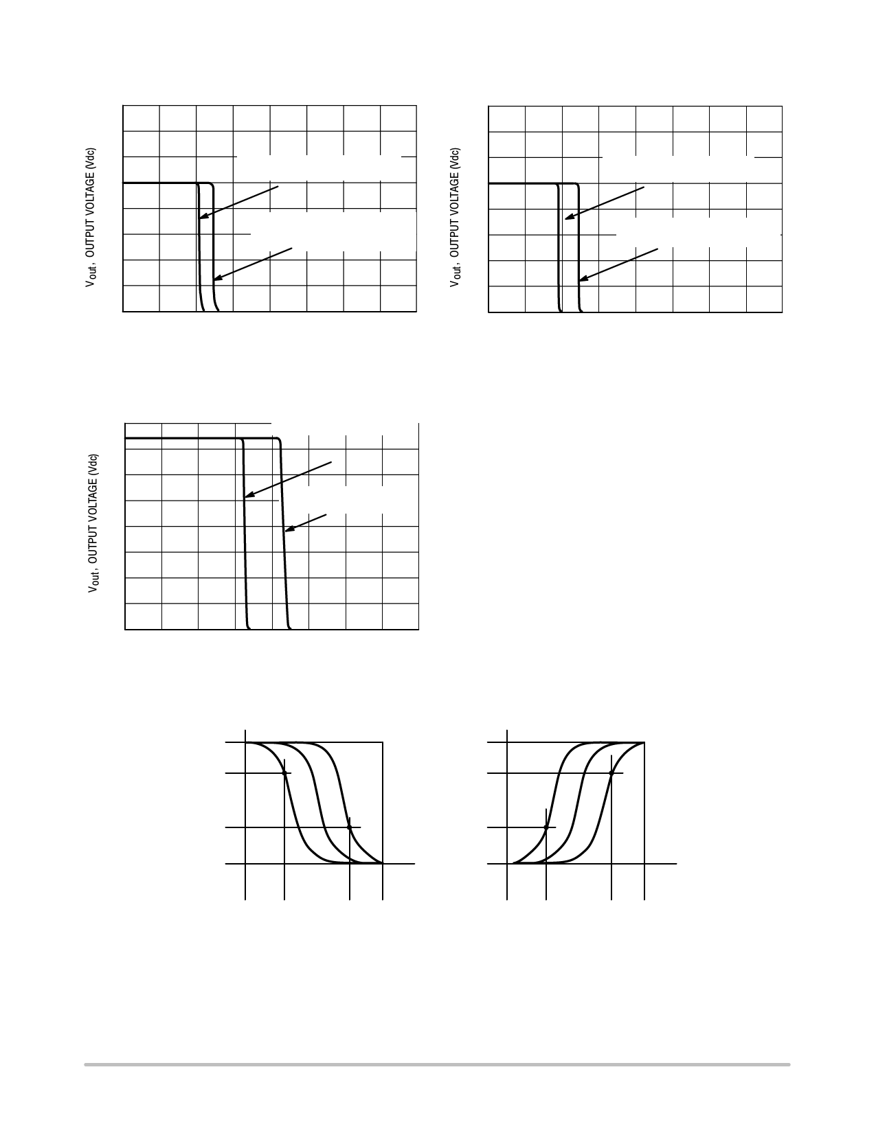
VOLTAGE TRANSFER CHARACTERISTICS
SINGLE INPUT NAND, AND
5.0
MULTIPLE INPUT NOR, OR
4.0
SINGLE INPUT NOR, OR
3.0
MULTIPLE INPUT NAND, AND
2.0
1.0
0
0 1.0 2.0 3.0 4.0 5.0
Vin, INPUT VOLTAGE (Vdc)
Figure 11. VDD = 5.0 Vdc
10
8.0
6.0
4.0
2.0
0
0
SINGLE INPUT NAND, AND
MULTIPLE INPUT NOR, OR
SINGLE INPUT NOR, OR
MULTIPLE INPUT NAND, AND
2.0 4.0 6.0 8.0 10
Vin, INPUT VOLTAGE (Vdc)
Figure 12. VDD = 10 Vdc
SINGLE INPUT NAND, AND
16
MULTIPLE INPUT NOR, OR
14
12
10
SINGLE INPUT NOR, OR
MULTIPLE INPUT NAND, A
8.0
6.0
4.0
2.0
0
0
2.0 4.0 6.0 8.0 10
Vin, INPUT VOLTAGE (Vdc)
Figure 13. VDD = 15 Vdc
DC NOISE MARGIN
The DC noise margin is defined as the input voltage range
from an ideal “1” or “0” input level which does not produce
output state change(s). The typical and guaranteed limit
values of the input values VIL and VIH for the output(s) to
be at a fixed voltage VO are given in the Electrical
Characteristics table. VIL and VIH are presented graphically
in Figure 11.
Guaranteed minimum noise margins for both the “1” and
“0” levels =
1.0 V with a 5.0 V supply
2.0 V with a 10.0 V supply
2.5 V with a 15.0 V supply
Vout
VDD
VO
Vout VDD
VO
VO
0
VDD
Vin
VO
0
VDD
Vin
VIL
VIH
(a) Inverting Function
VIL
VIH
VSS = 0 VOLTS DC
(b) Non−Inverting Function
Figure 14. DC Noise Immunity
http://onsemi.com
6
Share Link: 