AD7701 查看數據表(PDF) - Analog Devices
零件编号
产品描述 (功能)
比赛名单
AD7701 Datasheet PDF : 20 Pages
| |||
INPUT SIGNAL CONDITIONING
Reference voltages from 1 V to 3 V may be used with the AD7701
with little degradation in performance. Input ranges that cannot
be accommodated by this range of reference voltages may be
achieved by input signal conditioning. This may take the form
of gain to accommodate a smaller signal range, or passive attenua-
tion to reduce a larger input voltage range.
Source Resistance
If passive attenuators are used in front of the AD7701, care must
be taken to ensure that the source impedance is sufficiently low.
The AD7701 has an analog input with over 1 GΩ dc input
resistance. In parallel with this, there is a small dynamic load that
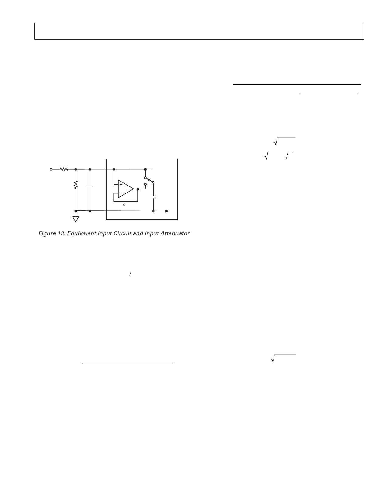
varies with the clock frequency (see Figure 13). Each time the
analog input is sampled, a 10 pF capacitor draws a charge packet
of maximum 1 pC (10 pF × 100 mV) from the analog source
R1
AIN
R2
CEXT
AGND
V OS 100mV
AD7701
CIN
10pF
Figure 13. Equivalent Input Circuit and Input Attenuator
with a frequency fCLKIN/256. For a 4.096 MHz CLKIN, this
yields an average current draw of 16 nA. After each sample, the
AD7701 allows 62 clock periods for the input voltage to settle.
The equation that defines settling time is:
[ ] VO = VIN 1 − e−t RC
where
VO is the final settled value.
VIN is the value of the input signal.
R is the value of the input source resistance.
C is the 10 pF sample capacitor.
t is equal to 62/fCLKIN.
From this, the following equation can be developed, which
gives the maximum allowable source resistance, RS(MAX), for
an error of VE:
RS (MAX ) =
fCLKIN
62
×(10 pF ) × l n (100mV
/VE )
Provided the source resistance is less than this value, the analog
input will settle within the desired error band in the requisite 62
clock periods. Insufficient settling leads to offset errors. These
can be calibrated in system calibration schemes.
If a limit of 10 µV (0.25 LSB at 16 bits) is set for the maximum
offset voltage, then the maximum allowable source resistance is
160 kΩ from the above equation, assuming that there is no
external stray capacitance.
AD7701
An RC filter may be added in front of the AD7701 to reduce
high frequency noise. With an external capacitor added from
AIN to AGND, the following equation will specify the maximum
allowable source resistance:
62
RS (Max) =
f CLKIN
× (CIN
+ CEXT
100
) × ln
mV
×
CIN / (CIN
VE
+ CEXT
)
The practical limit to the maximum value of source resistance is
thermal (Johnson) noise. A practical resistor may be modeled as
an ideal (noiseless) resistor in series with a noise voltage source
or in parallel with a noise current source:
Vn = 4kTRf Volts
in = 4kTRf R Amperes
where
k is Boltzmann’s constant (1.38 × 10⁻²³ J/K).
T is temperature in degrees Kelvin (°C + 273).
Active signal conditioning circuits such as op amps generally do
not suffer from problems of high source impedance. Their open-
loop output resistance is normally only tens of ohms and, in any
case, most modern general-purpose op amps have sufficiently
fast closed-loop settling time for this not to be a problem. Offset
voltage in op amps can be eliminated in a system calibration
routine. With the wide dynamic range and small LSB size of the
AD7701, noise can also be a problem, but the digital filter will
reject most broadband noise above its cutoff frequency. How-
ever, in certain applications there may be a need for analog
input filtering.
Antialias Considerations
The digital filter of the AD7701 does not provide any rejection
at integer multiples of the sampling frequency (nfCLKlN/256,
where n = 1, 2, 3 . . . ).
With a 4.096 MHz master clock, there are narrow (± 10 Hz)
bands at 16 kHz, 32 kHz, 48 kHz, and so on, where noise
passes unattenuated to the output.
However, due to the AD7701’s high oversampling ratio of 800
(16 kHz to 20 Hz), these bands occupy only a small fraction of
the spectrum and most broadband noise is filtered. The reduc-
tion in broadband noise is given by:
eOUT = eIN 2 f C / f S = 0.035 eIN
where
elN and eOUT are rms noise terms referred to the input.
fC is the filter –3 dB corner frequency (fCLKIN/409600).
fS is the sampling frequency (fCLKIN/256).
Since the ratio of fS to fCLKIN is fixed, the digital filter reduces
broadband white noise by 96.5% independent of the master
clock frequency.
REV. E
–11–
Share Link: 