MT9162 查看數據表(PDF) - Mitel Networks
零件编号
产品描述 (功能)
比赛名单
MT9162 Datasheet PDF : 17 Pages
| |||
MT9162
Advance Information
CSL2 CSL1 CSL0
External
Clock Bit
Rate (kHz)
CLOCKin
(kHz)
1
0
0
128
4096
1
0
1
256
4096
0
0
0
512
512
0
0
1
1536
1536
0
1
0
2048
2048
0
1
1
4096
4096
Table 2: Bit Clock Rate Selection
TxMute pin is high. When either of these pins are low
their respective paths function normally. The -Zero
entry of Table 1 is used for the quiet code definition.
SSI Mode
The SSI BUS consists of input and output serial data
streams named Din and Dout respectively, a Clock
input signal (CLOCKin), and a framing strobe input
(STB). A 4.096 MHz master clock is also required for
SSI operation if the bit clock is less than 512 kHz.
The timing requirements for SSI are shown in
Figures 5 & 6.
In SSI mode the MT9162 supports only B-Channel
operation. Hence, in SSI mode transmit and receive
B-Channel data are always in the channel defined by
the STB input.
The data strobe input STB determines the 8-bit
timeslot used by the device for both transmit and
receive data. This is an active high signal with an 8
kHz repetition rate.
SSI operation is separated into two categories based
upon the data rate of the available bit clock. If the bit
clock is 512 kHz or greater then it is used directly by
the internal MT9162 functions allowing synchronous
operation. If the available bit clock is 128 kHz or 256
kHz, then a 4096 kHz master clock is required to
derive clocks for the internal MT9162 functions.
Applications where Bit Clock (BCL) is below 512 kHz
are designated as asynchronous. The MT9162 will
re-align its internal clocks to allow operation when
the external master and bit clocks are asynchronous.
Control pins CSL2, CSL1 and CSL0 are used to
program the bit rates.
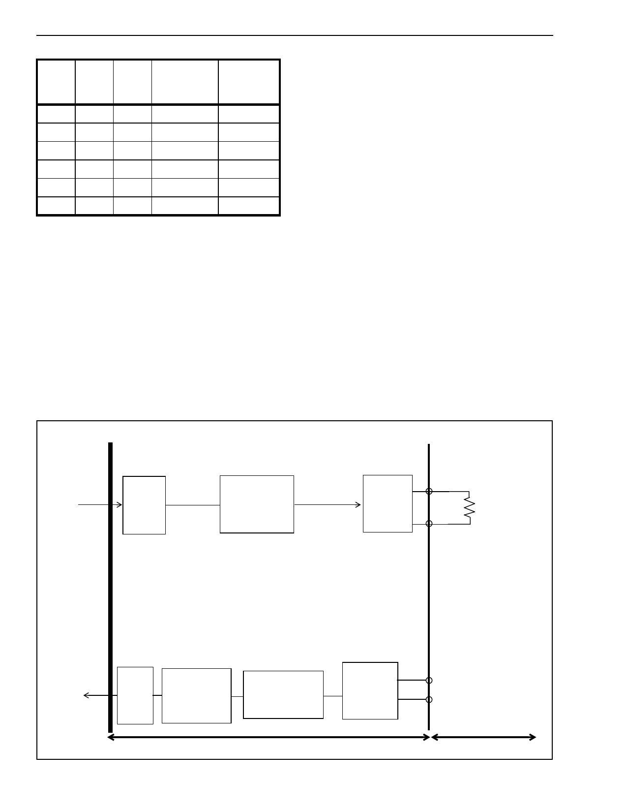
Serial Port
PCM
Din
Decoder
2.05 dB
Filter/Codec and Analog Interface
Receive
Filter Gain
0 dB
-2.05 dB
Receiver
Driver
Aout +
Aout-
20kΩ
PCM
Dout
7-164
Encoder
-2.05 dB
TTrraannssmmititFFiltieltrer
GGaainin
0 to0d+B7 dB
(1 dB steps)
Transmit Gain
-0.37 dB
Transmit
Gain
8.42 dB
Internal To Device
Figure 3 - Audio Gain Partitioning
AIN+ Analog
Input
AIN-
External To Device
Share Link: 