NJU3504FA1 查看數據表(PDF) - Japan Radio Corporation
零件编号
产品描述 (功能)
比赛名单
NJU3504FA1 Datasheet PDF : 60 Pages
| |||
NJU3504
• PORTB(PB0 − PB3)
PORTB is a 4-bit programmable input-output PORT. It is set as the output when the second bit (b1) of
the programmable input/output control register(PHY29) is set to “1”, and is set as the input when “b1” of
PHY29 is set to “0”. When the PORT is set as the output, the 4-bit signals are output through the output
terminals by writing data into the peripheral register assigned for PORTB(PHY18). PHY18 as the output
register should be written the output data before the PORTB is set as the output by PHY29, because the
conditions of the output terminals are unknown while the output data is not written in PHY18. When this
PORT is set as the input, the 4-bit external signals are gotten directly through the input terminals by
reading data from PHY18. PHY18 can be written or read independent of the state of PHY29 as the input
or output.
Though the output circuit is Nch open drain type, the C-MOS input buffer is connected to the same
terminal. Therefore, the operating current of the chip by the short circuit current when the middle level
voltage between VDD and VSS is input to this terminal.
PORTB is set as the input in accordance with the state of PHY29 set to “0” on the “RESET” operation.
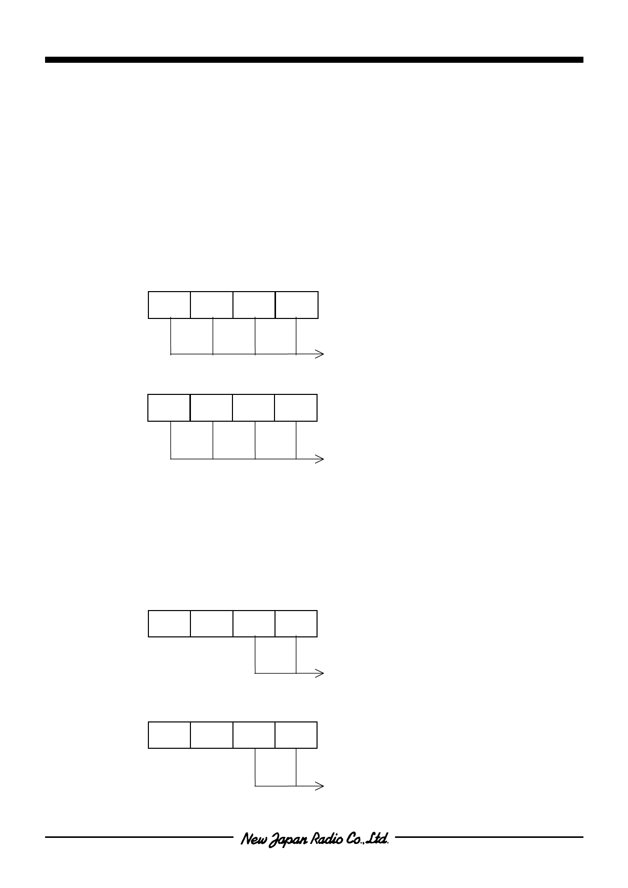
[READING PORTB INPUT DATA (PHY18)]
(MSB) 3
2
1
0
PHY18 PB3 PB2 PB1 PB0
(LSB)
[WRITING PORTB OUTPUT DATA (PHY18)]
(MSB) 3
2
1
0
PHY18 PB3 PB2 PB1 PB0
PORTB Input Data
(LSB)
PORTB Output Data
• PORTC(PC0, PC1)
PORTC is a 2-bit input-output PORT. The input or the output is selected for each bit by the mask
option. When the port is set as the output, the signal is output through the output terminal by writing data
to the PORTC register(PHY19). When the port is set as the input, the external signal is gotten directly
through the input terminal by reading data from PHY19.
Though the output circuit is Nch open drain type, the C-MOS input buffer is connected to the same
terminal. Therefore, the operating current of the chip by the short circuit current when the middle level
voltage between VDD and VSS is input to this terminal.
[READING PORTC INPUT DATA (PHY19)]
(MSB) 3
2
1
0
PHY19
“0”
“0” PC1 PC0
(LSB)
PORTC Input Data
[WRITING PORTC OUTPUT DATA (PHY19)]
(MSB) 3
2
1
0
PHY19
−
−
PC1 PC0
(LSB)
PORTC Output Data
- 16 -
Share Link: 