NJU6678CL 查看數據表(PDF) - Japan Radio Corporation
零件编号
产品描述 (功能)
比赛名单
NJU6678CL Datasheet PDF : 45 Pages
| |||
NJU6678
No
21
20
11
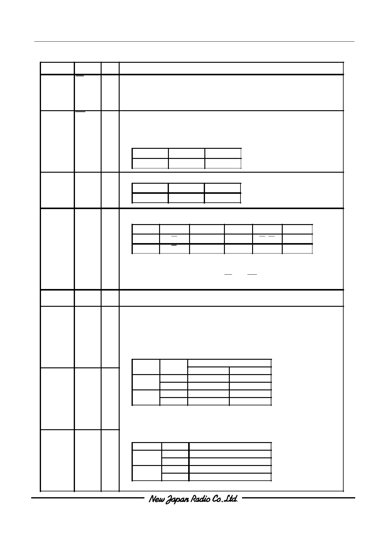
Symbol I/O
Function
RD(E)
I <In case of 80 Type MPU>
RD signal of 80 type MPU input terminal. Active "L"
During this signal is "L" , D0 to D7 terminals are output.
<In case of 68 Type MPU>
Enable signal of 68 type MPU input terminal. Active "H"
WR(RW) I <In case of 80 Type MPU>
Connect to the 80 type MPU WR signal. Actie "L".
The data on the data bus input syncronizing the rise edge of this signal.
<In case of 68 Type MPU>
The read/write control signal of 68 type MPU input terminal.
R/W
State
H
Read
L
Write
CEL68
I MPU interface type selection terminal.
CEL68
H
L
State
68 Type 80 Type
10
P/S
I serial or parallel interface selection terminal.
16
17
47 to 98
99 to 230
P/S
Chip Select Data/Command
Data
Read/Write serial Clock
"H"
CS
A
D 0 to D 7 RD,WR
-
"L"
CS
A0
SI(D7) Write Only SCL(D6)
RAM data and status read operation do not work in mode of
the serial interface.
In case of the serial interface (P/S="L"),RD and WR must be fixed
"H" or "L", and D0 to D5 are high impedance.
OSC1
OSC2
I System clock input terminal for Maker testing.(This terminal should be Open)
For external clock operation, the clock shoud be input to OSC1 terminal.
C0 to C51 O LCD driving signal output terminals.
Segmet output terminals:S 0 to S131
Common output terminals:C 0 to C1 0 3
Segment output terminal
The following output voltages are selected by the combination of FR and data in the
RAM.(non of the n-line inverse functions)
S0 to S1 3 1 O
RAM
Data
FR
H
H
L
H
L
L
Output Voltage
Normal
Reverse
V DD
V2
V5
V3
V2
V DD
V3
V5
282 to 231
C52 to
C103
Common output terminal
The following output voltages are selected by the combination of FR and status of
O common.
Scan data
FR
H
H
L
H
L
L
Output Voltage
V5
VDD
V1
V4
Share Link: 