NLAS1053 查看數據表(PDF) - ON Semiconductor
零件编号
产品描述 (功能)
比赛名单
NLAS1053 Datasheet PDF : 10 Pages
| |||
NLAS1053
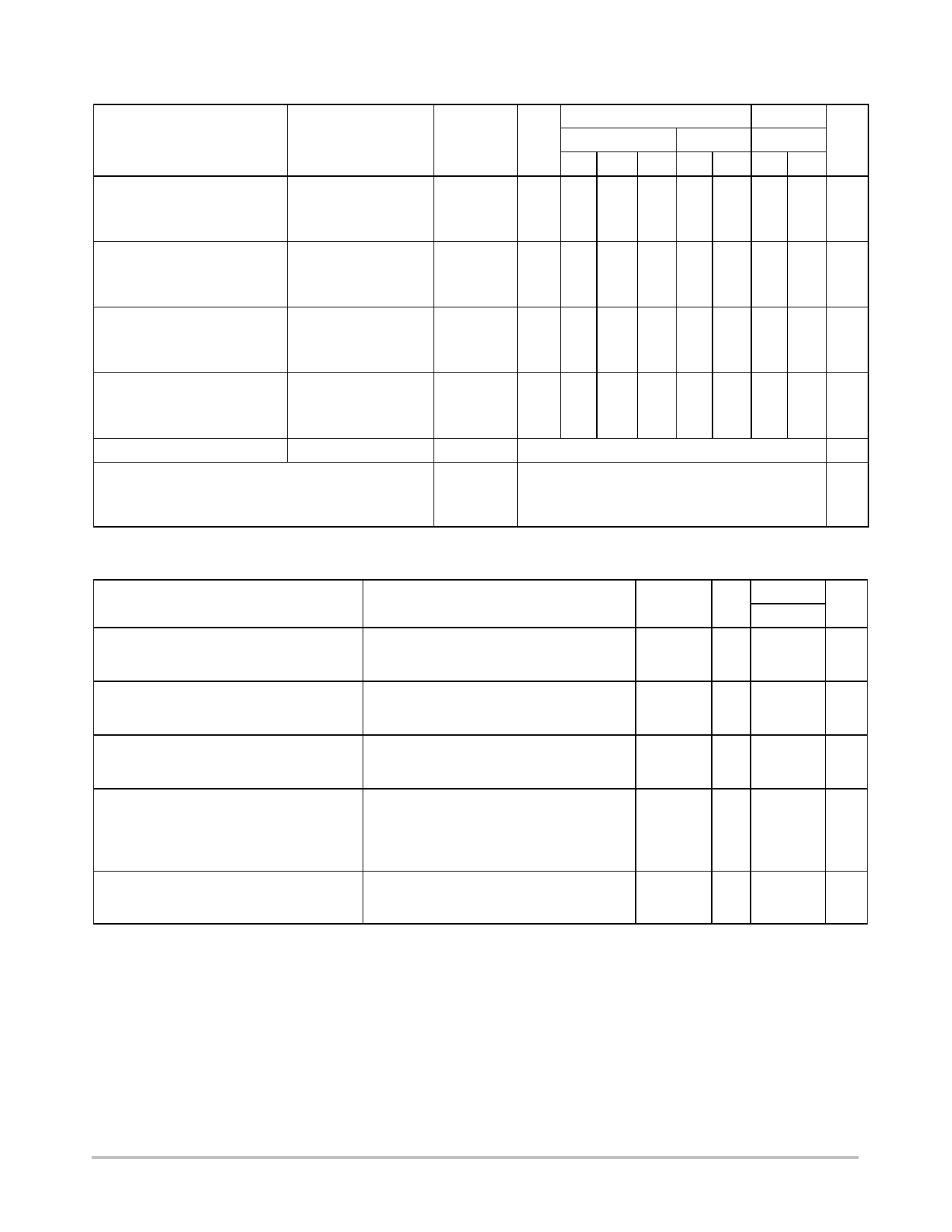
AC ELECTRICAL CHARACTERISTICS (Input tr = tf = 3.0 ns)
Guaranteed Max Limit
Parameter
Test Conditions
Symbol
VCC
-55 to 25_C
< 85_C < 125_C
(V) Min Typ* Max Min Max Min Max Unit
Turn−On Time
(Figures 12 and 13)
INH to Output
RL = 300 W, CL = 35 pF
tON
(Figures 4 and 5)
2.5 2 7 12 2 15 2 15 ns
3.0 2 5 10 2 15 2 15
4.5 1
4
9
1 12 1 12
5.5 1
3
8
1 12 1 12
Turn−Off Time
(Figures 12 and 13)
INH to Output
RL = 300 W, CL = 35 pF
tOFF
(Figures 4 and 5)
2.5 2 7 12 2 15 2 15 ns
3.0 2 5 10 2 15 2 15
4.5 1
4
9
1 12 1 12
5.5 1
3
8
1 12 1 12
Transition Time (Channel Selec-
tion Time)
(Figure )
Select to Output
RL = 300 W, CL = 35 pF
(Figures and )
ttrans
2.5 5 18 28 5 30 5 30 ns
3.0 5 13 21 5 25 5 25
4.5 2 12 16 2 20 2 20
5.5 2 9 14 2 20 2 20
Minimum
VIS = 3.0 V (Figure 3)
tBBM
2.5 1 12
1
1
ns
Break−Before−Make Time
RL = 300 W, CL = 35 pF
3.0 1 11
1
1
4.5 1 6
1
1
5.5 1 5
1
1
Typical @ 25, VCC = 5.0 V
Maximum Input Capacitance, Select/INH Input
CIN
8
pF
Analog I/O (switch off)
CNO or CNC
10
Common I/O (switch off)
CCOM
10
Feedthrough (switch on)
C(ON)
20
*Typical Characteristics are at 25_C.
ADDITIONAL APPLICATION CHARACTERISTICS (Voltages Referenced to GND Unless Noted)
ÎÎÎÎÎÎÎÎ Parameter
ÎÎÎÎ Maximum On−Channel −3dB Bandwidth or
Minimum Frequency Response
ÎÎÎÎ (Figure 10)
ÎÎÎÎ Maximum Feedthrough On Loss
ÎÎÎÎÎÎÎÎ Off−Channel Isolation
ÎÎÎÎ (Figure 10)
ÎÎÎÎ Charge Injection Select Input to
ÎÎÎÎ Common I/O
ÎÎÎÎ (Figure 15)
ÎÎÎÎÎÎÎÎ Total Harmonic Distortion
THD + Noise
ÎÎÎÎÎÎÎÎ (Figure 14)
Condition
VIN = 0 dBm
VIN centered between VCC and GND
(Figure 7)
VIN = 0 dBm @ 100 kHz to 50 MHz
VIN centered between VCC and GND
(Figure 7)
f = 100 kHz; VIS = 1 V RMS
VIN centered between VCC and GND
(Figure 7)
VIN = VCC to GND, FIS = 20 kHz
tr = tf = 3 ns
RIS = 0 W, CL = 1000 pF
Q = CL * DVOUT
(Figure 8)
FIS = 20 Hz to 100 kHz, RL = Rgen = 600 W
CL = 50 pF
VIS = 5.0 VPP sine wave
VCC
Symbol V
BW
3.0
4.5
5.5
VONL
3.0
4.5
5.5
VISO
3.0
4.5
5.5
Q
3.0
5.5
THD
5.5
Typical
25°C
170
200
200
−3
−3
−3
−93
−93
−93
1.5
3.0
0.1
Unit
MHz
dB
dB
pC
%
http://onsemi.com
4
Share Link: 