TB62725 查看數據表(PDF) - Marktech Optoelectronics
零件编号
产品描述 (功能)
比赛名单
TB62725 Datasheet PDF : 15 Pages
| |||
TOSHIBA
T B 6 2 7 2 5 P / F / FN
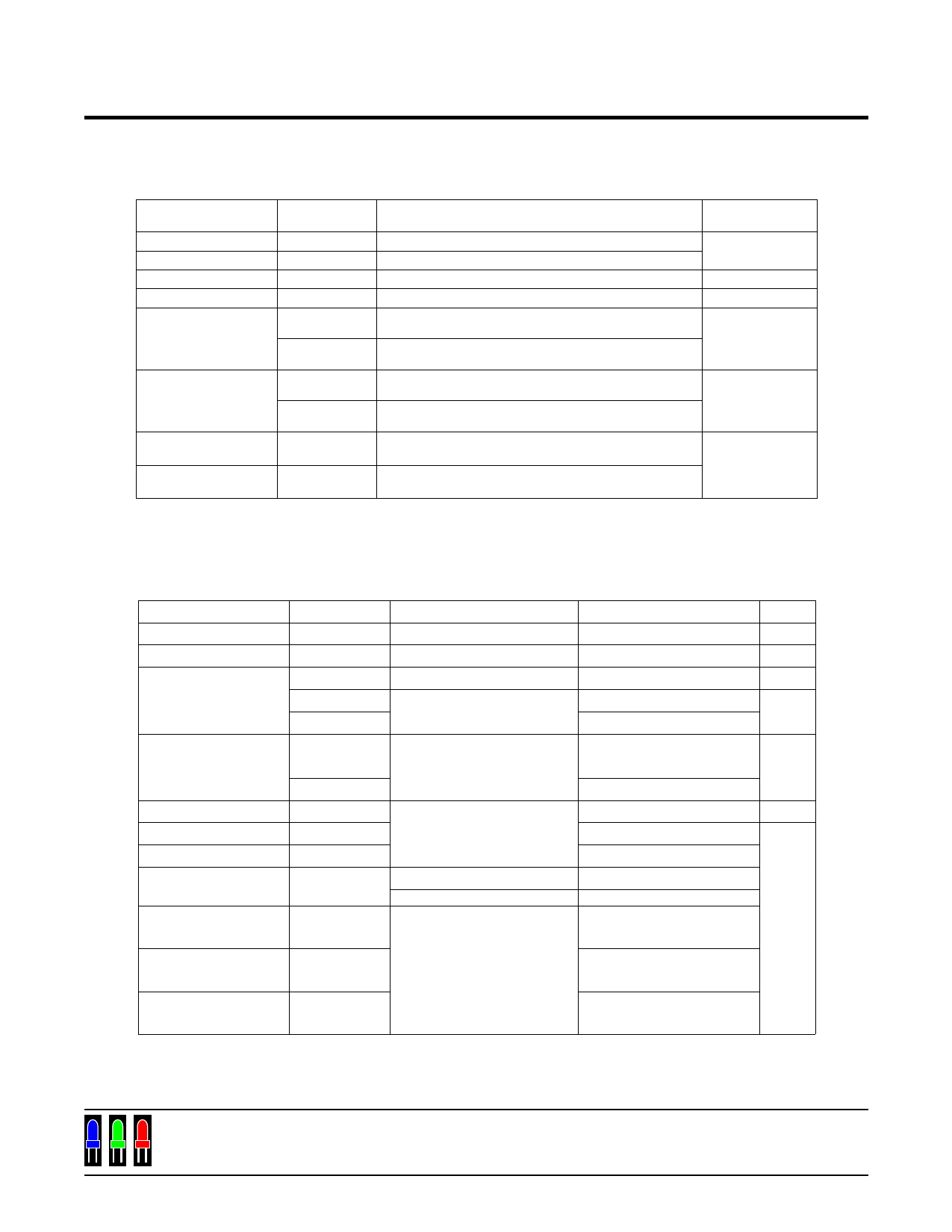
MAXIMUM RATINGS ( Ta = 25degC )
CHARACTERISTICS
SYMBOL
Supply Voltage
Input Voltage
Output Current
Output Voltage
Power Dissipation
VDD
VIN
IOUT
VOUT
Pd1
RATING
0 to 7
-0.2 to VDD+0.2
+90
-0.5 to 17
Type P : 1.47(Free Air)
UNIT
V
mA/ch
V
W
Pd2
Type F and FN : 0.37 (Free Air), 0.78 (On PCB)
Thrmal Resistance
Rth(j-a)1
Type P : 85(Free Air)
degC/W
Rth(j-a)2
Type F and FN : 330 (Free Air),160 (On PCB)
Oparating Temperature
Topr
-40 to 85
degC
Storage Temperature
Tstg
-55 to 150
Note) Type P : Ambient temperature delated above 25degC in the proportion of 11.76 mW/degC.
Type F and FN : Ambient temperature delated above 25degC in the proportion of 7.69 mW/degC.
Condition) On PCB at 50 X 50 X 1.6mm Cu <= 40% ( Glass Epoxy PCB )
RECOMMENDED OPERATING CONDITION (Ta=-40 to 85degC unless otherwise noted)
CHARACTERISTICS
Supply Voltage
Output Voltage
Output Current
SYMBOL
VDD
VOUT
IOUT
IOH
IOL
CONDITION
Each DC 1 Circuit
SERIAL-OUT
MIN.
3
2
TYP.
3.3
0.7
MAX.
3.6
4
70
-1
1
UNIT
V
V
mA/ch
mA
Input Voltage
VIH
0.7VDD
VDD
+0.15
V
Clock Frequency
/LATCH Pulse Width
CLOCK Pulse Width
/ENABLE Pulse Width
VIL
fCLK
tw /LATCH
tw CLOCK
tw /ENABLE
Setup Time
for CLOCK Terminal
tsetup1
Cascade Connected
Upper IOUT = 20 mA
Lower IOUT = 20 mA
-0.15
50
2000
4500
10
0.3VDD
20
MHz
25
ns
Hold Time
for CLOCK Terminal
thold
5
Setup Time
for /LATCH Terminal
tsetup2
50
marktech
optoelectronics
120 Broadway Menands, New York 12204
Toll Free: (800) 98-4LEDS Fax: (518) 432-7454
Share Link: 