TB62725 查看數據表(PDF) - Marktech Optoelectronics
零件编号
产品描述 (功能)
比赛名单
TB62725 Datasheet PDF : 15 Pages
| |||
TOSHIBA
T B 6 2 7 2 5 P / F / FN
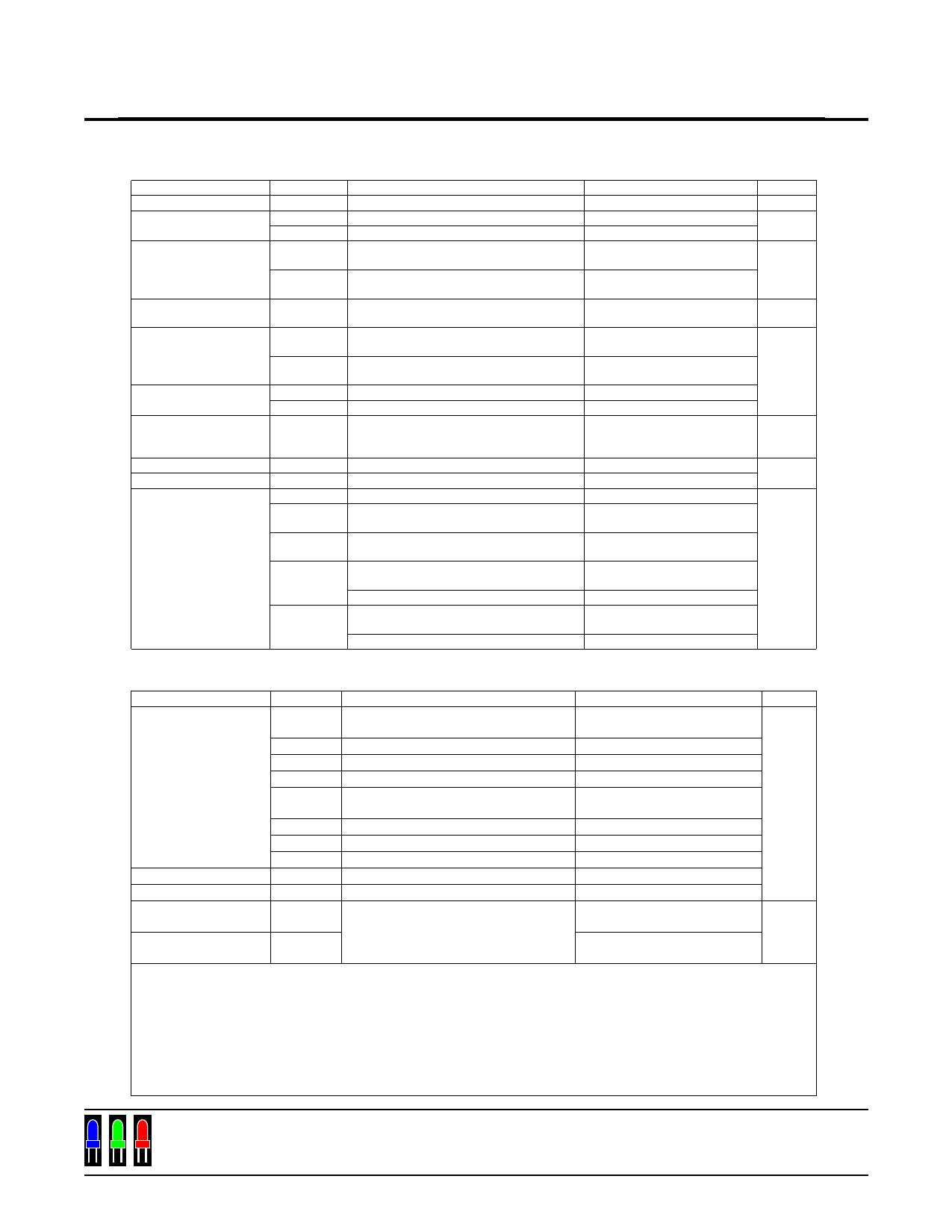
ELECTRICAL CHARACTERISTICS (VDD=3.3V, Ta=25degC unless otherwise noted)
CHARACTERISTICS
Supply Voltage
Output Current
Output Current
SYMBOL
VDD
IOUT1
IOUT2
dIOUT1
Error bitween bits
Output Leakage
Current
Input Voltage
dIOUT2
IOZ
VIH
SOUT Terminal
Output Voltage
Output Currnet
Supply Voltage
Reguration
Pull up Resistor
Pull down Resistor
VIL
VOL
VOH
%/VDD
R(up)
R(down)
IDD(OFF)1
IDD(OFF)2
Supply Current
IDD(OFF)3
IDD (O N)1
IDD (O N)2
CONDITION
Normal Operation
VOUT=0.4V,REXT=490ohms
VOUT=0.7V,REXT=250ohms
VOUT>=0.4V,REXT=490ohms
All outout on.
VOUT>=0.7V,REXT=250ohms
All outout on.
VOUT=15.0V
IOH=+1mA
IOL=-1mA
VDD = 3V to 3.6V
/ENABLE Terminal
/LATCH Terminal
REXT=OPEN,VOUT=15.0V
REXT=490Ohms,
VOUT=15V,OUT0 to 7 are Off.
REXT=250Ohms,
VOUT=15V,OUT0 to 7 are Off.
REXT=490Ohms,
VOUT=0.7V,OUT0 to 7 are On.
Same as the avobe , Ta=-40degC
REXT=250Ohms,
VOUT=0.7V,OUT0 to 7 are On.
Same as the avobe , Ta=-40degC
M IN
3.0
31.9
62.6
0.7
VDD
GND
2.8
100
125
1
3
TYP
3.3
37.5
73.6
+/-1.5
+/-1.5
1.0
+/-1.5
200
250
1
3
6
7
13
MAX
3.6
43.1
84.6
+/-6
+/-6
5.0
VDD
0.3
VDD
0.4
+/-5.0
400
500
2
5
8
14
25
UNIT
V
mA
%
uA
V
%
kohms
mA
SWITCHING CHARACTERISTICS (Ta=25degC unless otherwise noted)
CHARACTERISTICS SYBOL
TEST CONDITION
MIN
TYP
tpLH1
CLK - OUTn,
/LATCH="H",/ENABLE="L"
140
tpLH2
/LATCH - OUTn, /ENABLE="L"
140
tpLH3
/ENABLE - OUTn, /LATCH="H"
140
Propagation
tpLH
CLK - SERIAL OUT
5
Delay Time
tpHL1
CLK - OUTn,
/LATCH="H",/ENABLE="L"
170
tpHL2
/LATCH - OUTn, /ENABLE="L"
170
tpHL3
/ENABLE - OUTn, /LATCH="H"
170
tpHL
CLK - SERIAL OUT
6
Output Rise Time
t or
Voltage Waveform 10% to 90%
70
Output Fall Time
t of
Voltage Waveform 90% to 10%
90
Muximum CLOCK
Rise Time
tr
Cascade connection isn't guarantee.
Muximum CLOCK
Fall Time
tf
(Note1)
MAX UNIT
ns
5
us
5
Condition : (Refer to test circuit.)
Ta= 25 degC, VDD=VIH=3.3V, VOUT=0.7V, VIL=0V, REXT=490ohms, VL=3.0V, RL=60ohms, CL=10.5pF
Note 1 : When tf / tf of clock wave form is enlarged at the time as the cascade connection,
the timing condition which is necessary for the data transfer may not be able to be secured.
Give careful consideration to the timing condition.
marktech
optoelectronics
120 Broadway Menands, New York 12204
Toll Free: (800) 98-4LEDS Fax: (518) 432-7454
Share Link: 