PCF8584 查看數據表(PDF) - NXP Semiconductors.
零件编号
产品描述 (功能)
比赛名单
PCF8584 Datasheet PDF : 40 Pages
| |||
Philips Semiconductors
I2C-bus controller
Product specification
PCF8584
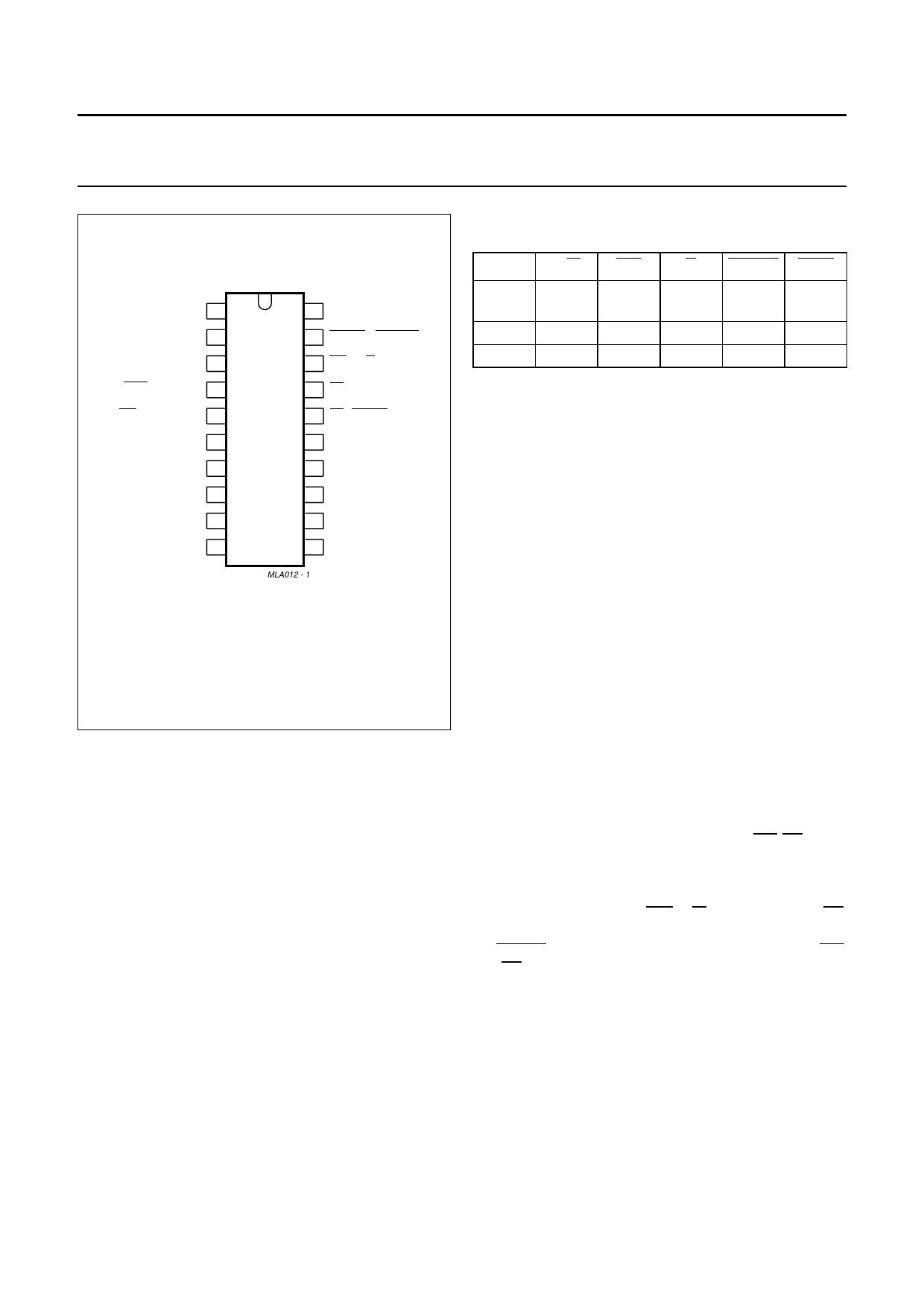
handbook, halfpage
CLK 1
SDA or SDA OUT 2
SCL or SCL IN 3
20 VDD
19 RESET / STROBE
(1)
18 WR (R/W)
IACK or SDA IN 4
INT or SCL OUT 5
A0 6
PCF8584
17 CS
(1)
16 RD (DTACK)
15 DB7
DB0 7
14 DB6
DB1 8
13 DB5
DB2 9
VSS 10
12 DB4
11 DB3
MLA012 - 1
(1) Pin mnemonics between parenthesis indicate the 68000 mode
pin designations.
Fig.2 Pin configuration.
6 FUNCTIONAL DESCRIPTION
6.1 General
The PCF8584 acts as an interface device between
standard high-speed parallel buses and the serial I2C-bus.
On the I2C-bus, it can act either as master or slave.
Bidirectional data transfer between the I2C-bus and the
parallel-bus microcontroller is carried out on a byte-wise
basis, using either an interrupt or polled handshake.
Interface to either 80XX-type (e.g. 8048, 8051, Z80) or
68000-type buses is possible. Selection of bus type is
automatically performed (see Section 6.2).
Table 1 Control signals utilized by the PCF8584 for
microcontroller/microprocessor interfacing
TYPE R/W WR
R DTACK IACK
8048/
no
yes
yes
no
no
8051
68000 yes
no
no
yes
yes
Z80
no
yes
yes
no
yes
The structure of the PCF8584 is similar to that of the
I2C-bus interface section of the Philips’
MABXXXX/PCF84(C)XX-series of microcontrollers, but
with a modified control structure. The PCF8584 has five
internal register locations. Three of these (own address
register S0', clock register S2 and interrupt vector S3) are
used for initialization of the PCF8584. Normally they are
only written once directly after resetting of the PCF8584.
The remaining two registers function as double registers
(data buffer/shift register S0, and control/status
register S1) which are used during actual data
transmission/reception. By using these double registers,
which are separately write and read accessible, overhead
for register access is reduced. Register S0 is a
combination of a shift register and data buffer.
Register S0 performs all serial-to-parallel interfacing with
the I2C-bus.
Register S1 contains I2C-bus status information required
for bus access and/or monitoring.
6.2 Interface Mode Control (IMC)
Selection of either an 80XX mode or 68000 mode
interface is achieved by detection of the first WR-CS signal
sequence. The concept takes advantage of the fact that
the write control input is common for both types of
interfaces. An 80XX-type interface is default. If a
HIGH-to-LOW transition of WR (R/W) is detected while CS
is HIGH, the 68000-type interface mode is selected and
the DTACK output is enabled. Care must be taken that WR
and CS are stable after reset.
1997 Oct 21
6
Share Link: 