PCF8584 查看數據表(PDF) - NXP Semiconductors.
零件编号
产品描述 (功能)
比赛名单
PCF8584 Datasheet PDF : 40 Pages
| |||
Philips Semiconductors
I2C-bus controller
Product specification
PCF8584
6.3 Set-up registers S0', S2 and S3
Registers S0', S2 and S3 are used for initialization of the
PCF8584 (see Fig.5 ‘Initialization sequence’ flowchart).
6.4 Own address register S0'
When the PCF8584 is addressed as slave, this register
must be loaded with the 7-bit I2C-bus address to which the
PCF8584 is to respond. During initialization, the own
address register S0' must be written to, regardless
whether it is later used. The Addressed As Slave (AAS) bit
in status register S1 is set when this address is received
(the value in S0 is compared with the value in S0'). Note
that the S0 and S0' registers are offset by one bit; hence,
programming the own address register S0' with a value of
55H will result in the value AAH being recognized as the
PCF8584’s slave address (see Fig.1).
Programming of S0' is accomplished via the parallel-bus
when A0 is LOW, with the appropriate bit combinations set
in control status register S1 (S1 is written when
pin A0 = HIGH). Bit combinations for accessing all
registers are given in Table 5. After reset, S0' has default
address 00H (PCF8584 is thus initially in monitor mode,
see Section 6.12.3).
6.5 Clock register S2
Register S2 provides control over chip clock frequency
and SCL clock frequency. S20 and S21 provide a selection
of 4 different I2C-bus SCL frequencies which are shown in
Table 2. Note that these SCL frequencies are only
obtained when bits S24, S23 and S22 are programmed to
the correct input clock frequency (fclk).
Programming of S2 is accomplished via the parallel-bus
when A0 = LOW, with the appropriate bit combinations set
in control status register S1 (S1 is written when
A0 = HIGH). Bit combinations for accessing all registers
are given in Table 5.
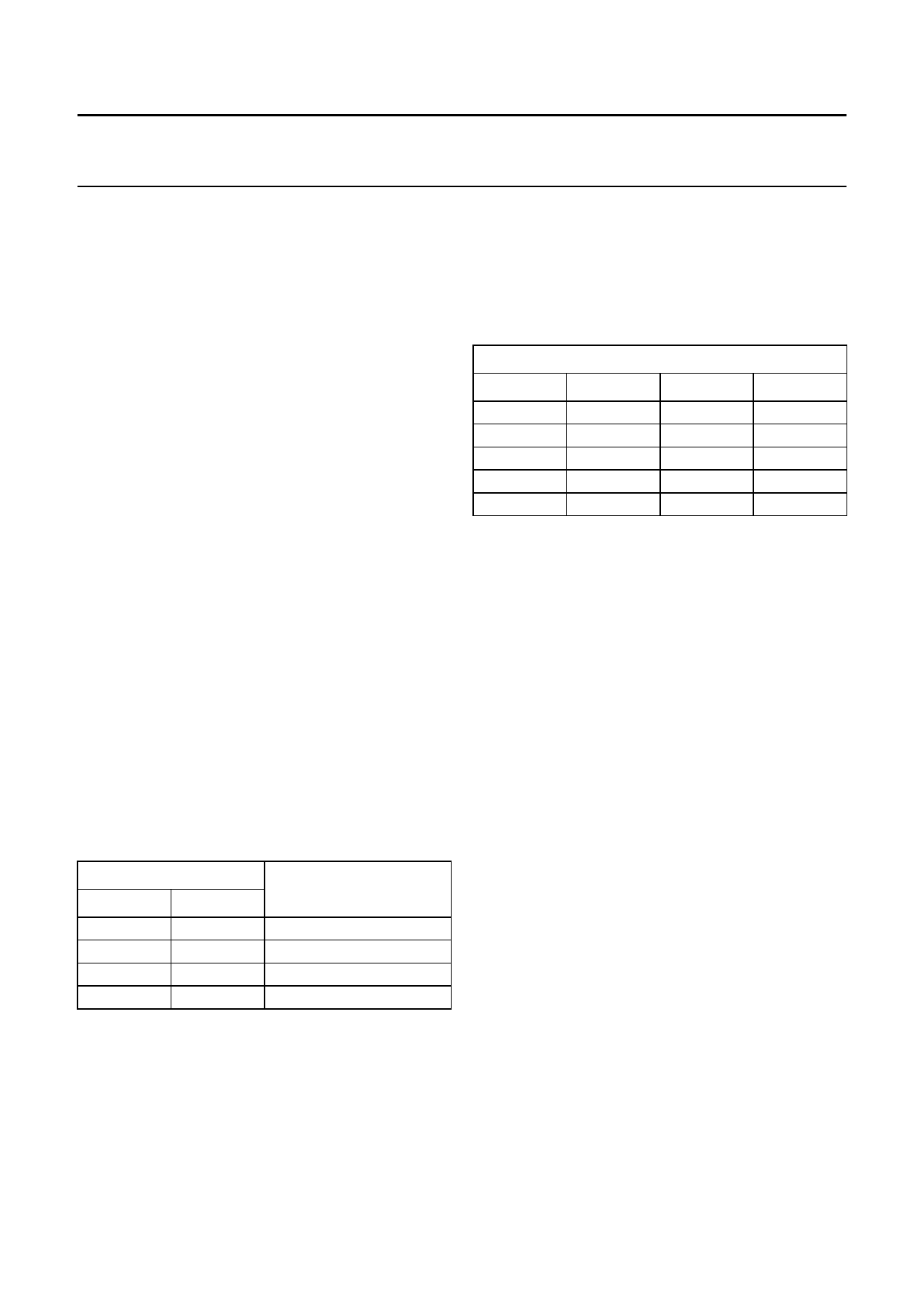
Table 3 Register S2 selection of clock frequency
INTERNAL CLOCK FREQUENCY
S24
S23
S22
fclk (MHz)
0
X(1)
X(1)
3
1
0
0
4.43
1
0
1
6
1
1
0
8
1
1
1
12
Note
1. X = don’t care.
6.6 Interrupt vector S3
The interrupt vector register provides an 8-bit
user-programmable vector for vectored-interrupt
microcontrollers. The vector is sent to the bus port
(DB7 to DB0) when an interrupt acknowledge signal is
asserted and the ENI (enable interrupt) flag is set. Default
vector values are:
• Vector is ‘00H’ in 80XX mode
• Vector is ‘0FH’ in 68000 mode.
On reset the PCF8584 is in the 80XX mode, thus the
default interrupt vector is ‘00H’.
Table 2 Register S2 selection of SCL frequency
BIT
S21
S20
0
0
0
1
1
0
1
1
APPROXIMATE SCL
FREQUENCY fSCL (kHz)
90
45
11
1.5
6.7 Data shift register/read buffer S0
Register S0 acts as serial shift register and read buffer
interfacing to the I2C-bus. All read and write operations
to/from the I2C-bus are done via this register. S0 is a
combination of a shift register and a data buffer; parallel
data is always written to the shift register, and read from
the data buffer. I2C-bus data is always shifted in or out of
shift register S0.
S22, S23 and S24 are used for control of the internal clock
prescaler. Due to the possibility of varying microcontroller
clock signals, the prescaler can be programmed to adapt
to 5 different clock rates, thus providing a constant internal
clock. This is required to provide a stable time base for the
SCL generator and the digital filters associated with the
I2C-bus signals SCL and SDA. Selection for adaption to
external clock rates is shown in Table 3.
1997 Oct 21
8
Share Link: 