LC86E6548 查看數據表(PDF) - SANYO -> Panasonic
零件编号
产品描述 (功能)
比赛名单
LC86E6548 Datasheet PDF : 21 Pages
| |||
LC86E6548
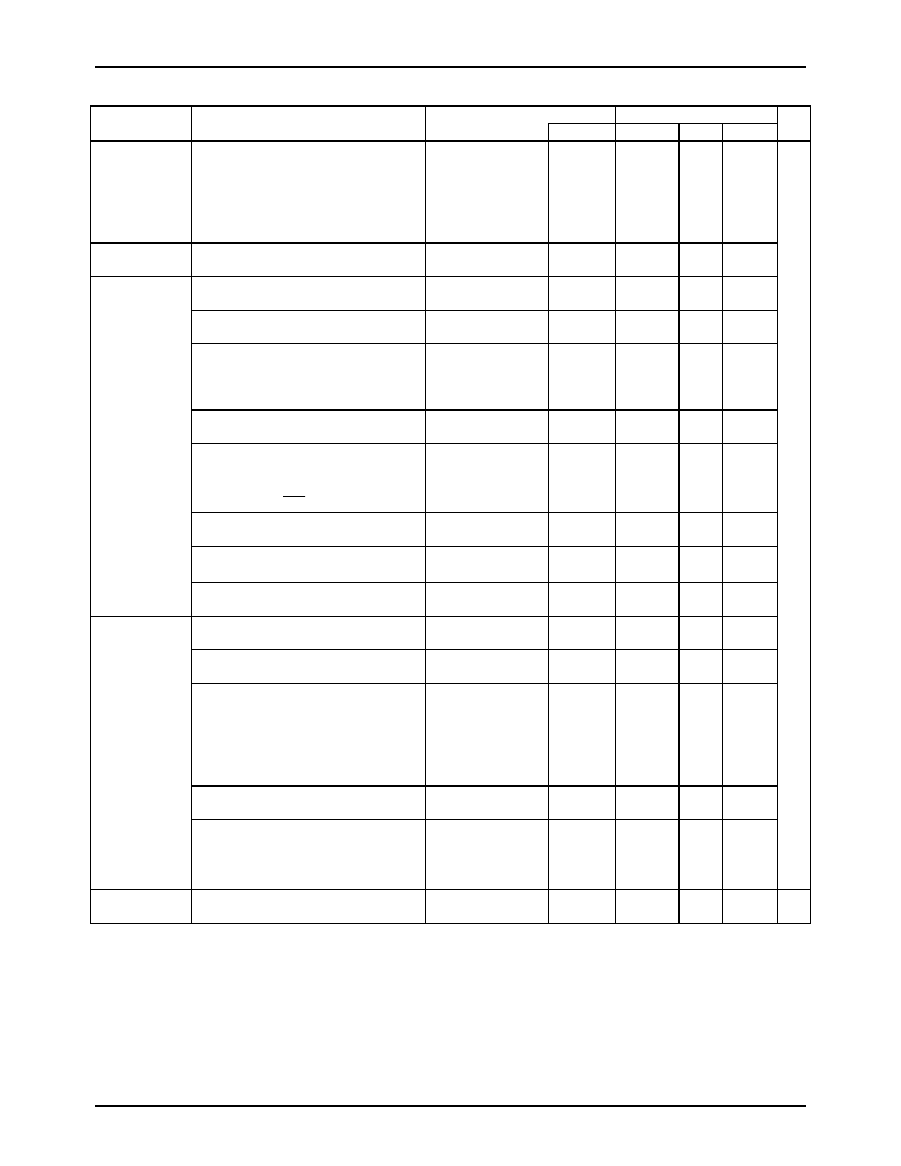
2. Recommended Operating Range at Ta=+10°C to +40°C, VSS1=VSS2=0V
Parameter
Symbol
Operating
VDD(1)
Supply voltage
Hold voltage VHD
Pull-down
Voltage
Input high
voltage
VP
VIH(1)
VIH(2)
VIH(3)
VIH(4)
VIH(5)
Input low
voltage
VIH(6)
VIH(7)
VIH(8)
VIL(1)
VIL(2)
VIL(3)
VIL(4)
Operation
cycle time
VIL(5)
VIL(6)
VIL(7)
tCYC
Pins
VDD1=VDD2
=VVDD3=VDD4
VDD1=VDD2
VP
Conditions
0.98µs ≤ tCYC
tCYC ≤ 400µs
RAMs and the
registers hold
voltage at HOLD
mode.
Port 0 at CMOS output Output disable
Port 0 at N-ch open drain
output
•Port 1
•Ports 72,73
•Port 3 at CMOS
output
•Port 3 at N-ch open
drain output
•Port 70
Port input/interrupt
•Port 71
• RES
Port 70
Watchdog timer
•Port 8
•Ports 74 ,75
S16 to S51
Port 0 at CMOS
output option
Port 0 at N-ch open
drain output
•Ports 1,3
•Ports 72,73
•Port 70
Port input/interrupt
•Port 71
• RES
Port 70
Watchdog timer
•Port 8
•Ports 74 ,75
S16 to S51
Output disable
Output disable
Output disable
Tr. OFF
Output disable
Output disable
Output disable
Output P-channel
Tr. OFF
Output disable
Output disable
Output disable
Output disable
Output disable
Output disable
Output P-channel
Tr. OFF
Continue.
VDD[V]
Ratings
min. typ.
max.
unit
4.5
6.0 V
2.0
6.0
4.5 to 6.0 -35
4.5 to 6.0 0.33VDD
+1.0
4.5 to 6.0 0.75VDD
4.5 to 6.0 0.75VDD
VDD
VDD
13.5
VDD
4.5 to 6.0 0.75VDD
4.5 to 6.0 0.75VDD
13.5
VDD
4.5 to 6.0 0.9VDD
4.5 to 6.0 0.75VDD
4.5 to 6.0 0.33VDD
+1.0
4.5 to 6.0 VSS
4.5 to 6.0 VSS
4.5 to 6.0 VSS
4.5 to 6.0 VSS
VDD
VDD
VDD
0.2VDD
0.25VDD
0.25VDD
0.25VDD
4.5 to 6.0 VSS
4.5 to 6.0 VSS
4.5 to 6.0 VP
4.5 to 6.0 0.98
0. 8VDD
-1.0
0.25VDD
0.2VDD
400 µs
No.6747-11/21
Share Link: 