LC86E6548 查看數據表(PDF) - SANYO -> Panasonic
零件编号
产品描述 (功能)
比赛名单
LC86E6548 Datasheet PDF : 21 Pages
| |||
LC86E6548
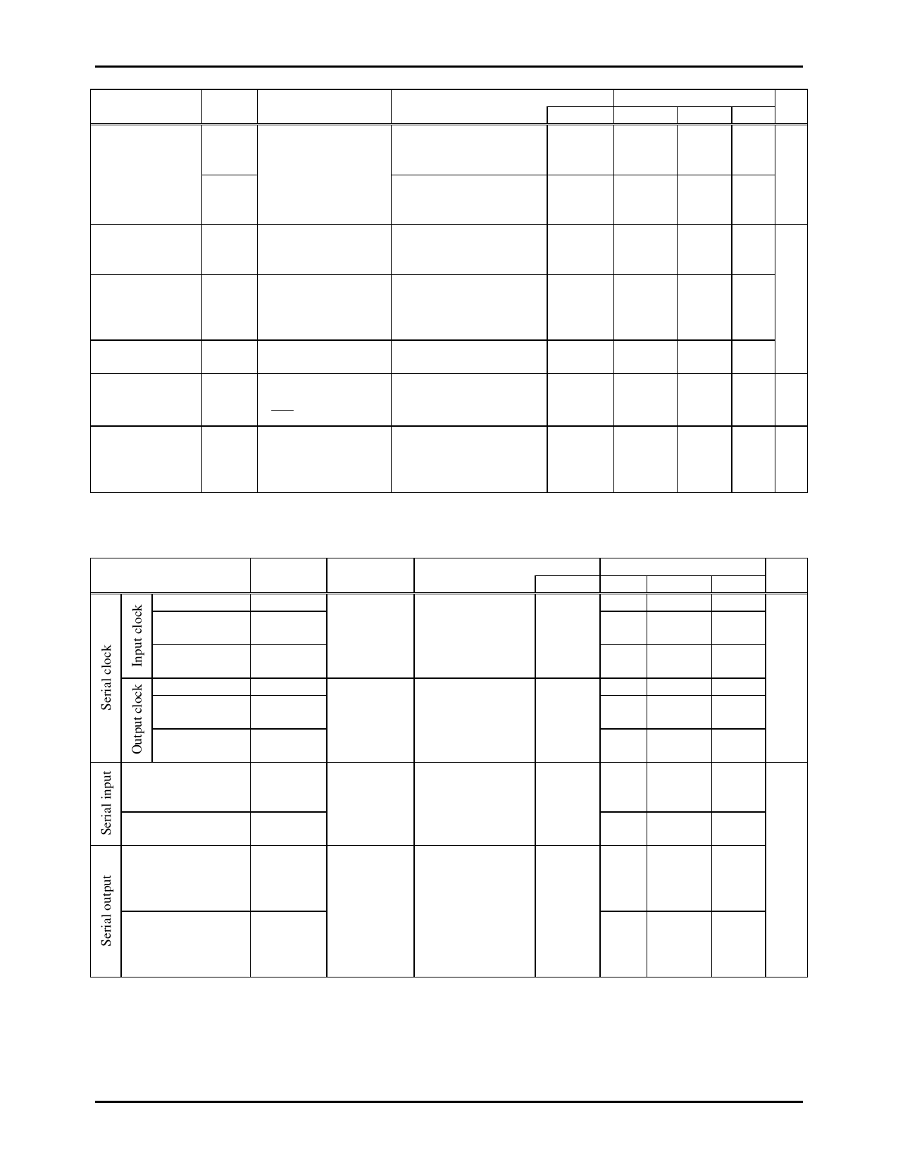
Parameter
Output off-
leakage current
Resistance of
The low level
Hold Tr.
High voltage
Pull-down
resistor
VP pull-down
resistor
Hysteresis
voltage
Pin capacitance
Symbol
Pins
Conditions
IOFF(1) •S0/T0 to S6/T6
•S32 to S51
(without pull-down
IOFF(2) resistor)
Rinpd S16 to S51
Rpd •S7/T7 to S15/T15
•S16 to S31
Rvppd Vp
VHIS
CP
•Port 1
•Ports 70,71,72,73,75
• RES
All pins
•Output P-channel
Tr. OFF
•VOUT=VSS
•Output P-channel
Tr. OFF
•VOUT=VDD-40V
•Output P-channel
Tr. OFF
•Using as input ports
•Output P-channel
Tr. OFF
•VOUT=3V
•Vp=-30V
•VSS=GND
•Vp=-30V
Output disable
•f=1MHz
•VIN=VSS for all
unmeasured terminals.
•Ta=25°C
VDD[V]
4.5 to 6.0
4.5 to 6.0
4.5 to 6.0
5.0
5.0
4.5 to 6.0
4.5 to 6.0
Ratings
min.
typ.
-1
max. unit
µA
-30
200
kΩ
60
100 200
60
100 200
0.1VDD
V
10
pF
4. Serial Input / Output Characteristics at Ta=+10°C to +40°C, VSS1=VSS2=0V
Parameter
Cycle
Low Level
pulse width
High Level
pulse width
Cycle
Low Level
pulse width
High Level
pulse width
Data set-up time
Data hold time
Output delay time
(External clock
using for serial
transfer clock)
Output delay time
(Internal clock
using for serial
transfer clock)
Symbol
Pins
Conditions
tCKCY(1) SCK0,SCK1 Refer to figure 5
tCKL(1)
VDD[V] min.
4.5 to 6.0 2
1
Ratings
typ.
max. unit
tCYC
tCKH(1)
1
tCKCY(2) SCK0,SCK1 •Use pull-up
4.5 to 6.0 2
tCKL(2)
resistor (1kΩ) in
1/2tCKCY
the open drain
tCKH(2)
output.
1/2tCKCY
•Refer to figure 5
tICK
•SI0,SI1
•Data set-up to
4.5 to 6.0 0.1
µs
•SB0,SB1
SCK0,1
•Data hold from
tCKI
SCK0,1
0.1
•Refer to figure 5
tCKO(1) •SO0,SO1 •Use pull-up
4.5 to 6.0
7/12
•SB0,SB1
resistor (1kΩ) in
the open drain
tCYC
+0.2
output.
tCKO(2)
•Data hold from
1/3
SCK0,1
tCYC
•Refer to figure 5
+0.2
No.6747-14/21
Share Link: 