LC86E6548 查看數據表(PDF) - SANYO -> Panasonic
零件编号
产品描述 (功能)
比赛名单
LC86E6548 Datasheet PDF : 21 Pages
| |||
LC86E6548
Pin name I/O
Function description
S48 to S51 I/O •Output for VFD display controller segment
-
*9
•Other function
S48 : High voltage I/O port PG0
S49 : High voltage I/O port PG1
S50 : High voltage I/O port PG2
S51 : High voltage I/O port PG3
RES
I Reset pin
-
XT1/ P74
I •Input pin for 32.768kHz crystal oscillation
-
•Other function
XT1 : Input port P74
In case of non use, connect to VDD1.
XT2/P75 O •Output pin for 32.768kHz crystal oscillation
-
•Other function
XT2 : Input port P75
In case of non use, connect to VDD1 at using
as port or unconnect at using as oscillation.
CF1
I Input pin for the ceramic resonator oscillation
-
CF2
O Output pin for the ceramic resonator oscillation
-
♦ All of port options (except pull-up resistor of port 0) can be specified in bit unit.
Option
*1 Memory select input for data security
*2 Output enable input
*3 Chip enable input
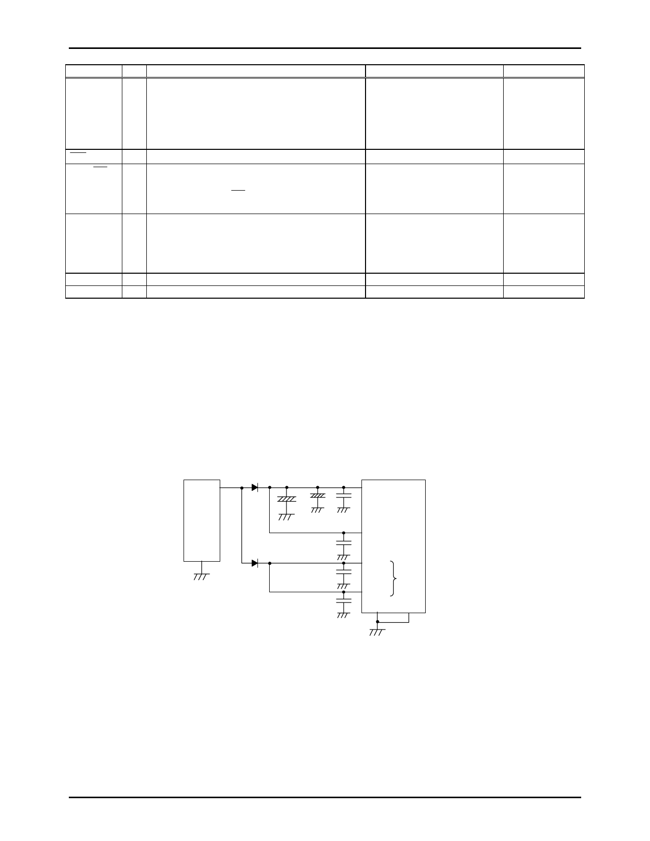
*4 Connect like the following figure to reduce noise into a VDD1 terminal.
Shorted the VSS1 terminal to the VSS2 terminal and to make the back-up time long.
*5 TA ! EPROM control signal input
*6 S0/T0 to S6/T6 : not provided the pull-down resistor
*7 S7/T7 to S15/T15 : provided the pull-down resistor (fixed)
*8 S16 to S31 : provided the pull-down resistor (fixed)
*9 S32 to S51 : not provided the pull-down resistor
Power
Supply
Back-up capacitor
LSI
VDD1
VDD2
VDD3
VDD4
VSS1
VFD
powers
VSS2
EPROM mode
-
-
-
-
-
-
No.6747-9/21
Share Link: 