PIC16C712 查看數據表(PDF) - Microchip Technology
零件编号
产品描述 (功能)
比赛名单
PIC16C712 Datasheet PDF : 108 Pages
| |||
PIC16C712/716
2.2 Data Memory Organization
The data memory is partitioned into multiple banks
which contain the General Purpose Registers and the
Special Function Registers. Bits RP1 and RP0 are the
bank select bits.
RP1(1) RP0
(STATUS<6:5>)
= 00 → Bank0
= 01 → Bank1
= 10 → Bank2 (not implemented)
= 11 → Bank3 (not implemented)
Note 1: Maintain this bit clear to ensure upward compati-
bility with future products.
Each bank extends up to 7Fh (128 bytes). The lower
locations of each bank are reserved for the Special
Function Registers. Above the Special Function Regis-
ters are General Purpose Registers, implemented as
static RAM. All implemented banks contain special
function registers. Some “high use” special function
registers from one bank may be mirrored in another
bank for code reduction and quicker access.
2.2.1 GENERAL PURPOSE REGISTER FILE
The register file can be accessed either directly, or indi-
rectly through the File Select Register FSR
(Section 2.5).
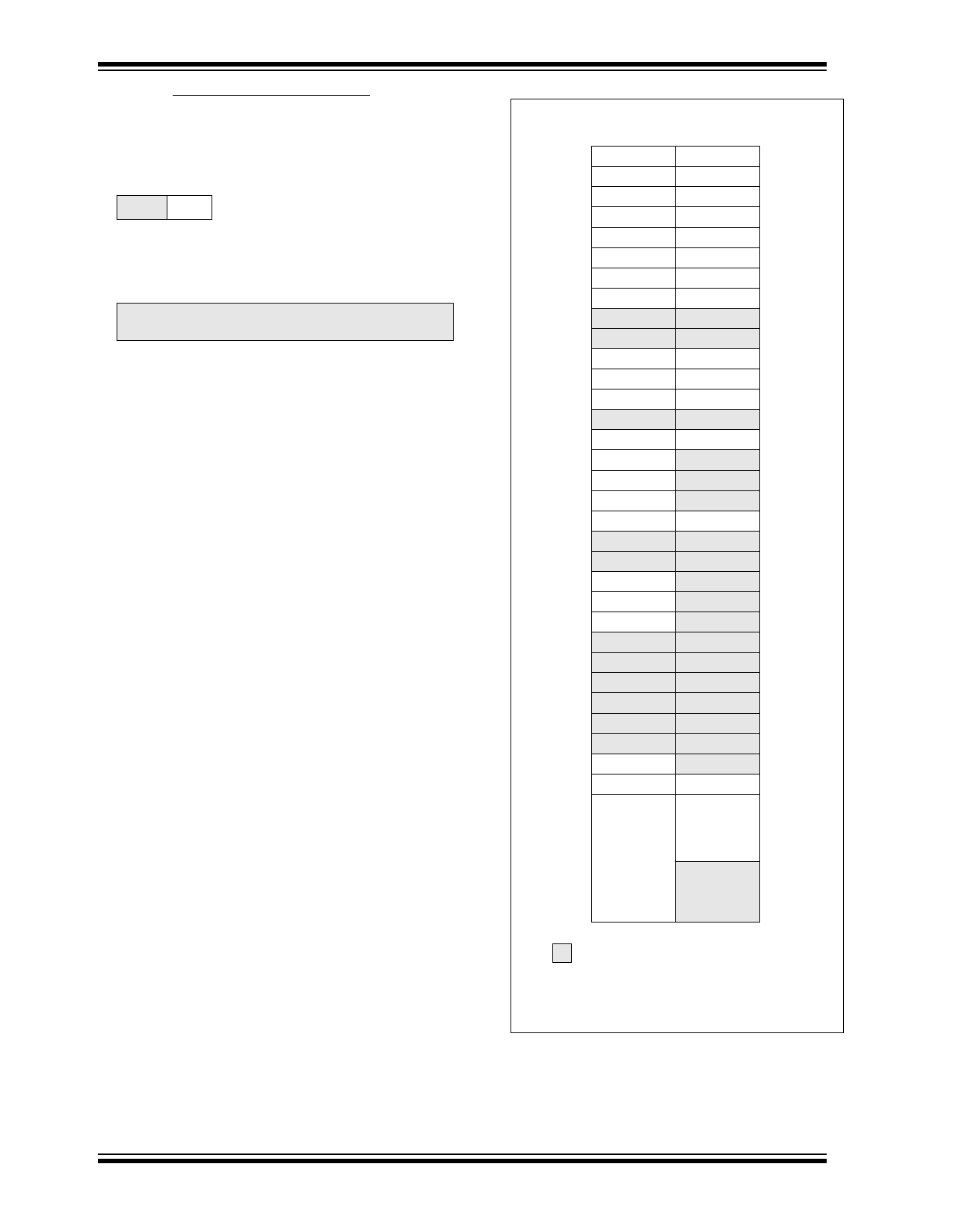
FIGURE 2-3: REGISTER FILE MAP
File
Address
00h
01h
02h
03h
04h
05h
06h
07h
08h
09h
0Ah
0Bh
0Ch
0Dh
0Eh
0Fh
10h
11h
12h
13h
14h
15h
16h
17h
18h
19h
1Ah
1Bh
1Ch
1Dh
1Eh
1Fh
20h
INDF(1)
TMR0
PCL
STATUS
FSR
PORTA
PORTB
DATACCP
PCLATH
INTCON
PIR1
TMR1L
TRM1H
T1CON
TRM2
T2CON
CCPR1L
CCPR1H
CCP1CON
ADRES
ADCON0
General
Purpose
Registers
96 Bytes
INDF(1)
File
Address
80h
OPTION_REG 81h
PCL
82h
STATUS 83h
FSR
84h
TRISA 85h
TRISB 86h
TRISCCP 87h
88h
89h
PCLATH 8Ah
INTCON 8Bh
PIE1
8Ch
8Dh
PCON 8Eh
8Fh
90h
91h
PR2
92h
93h
94h
95h
96h
97h
98h
99h
9Ah
9Bh
9Ch
9Dh
9Eh
ADCON1 9Fh
General A0h
Purpose
Registers
32 Bytes BFh
C0h
7Fh
FFh
Bank 0
Bank 1
Unimplemented data memory locations,
read as ’0’.
Note 1: Not a physical register.
DS41106A-page 10
Preliminary
© 1999 Microchip Technology Inc.
Share Link: 