PIC16C712 查看數據表(PDF) - Microchip Technology
零件编号
产品描述 (功能)
比赛名单
PIC16C712 Datasheet PDF : 108 Pages
| |||
PIC16C712/716
1.0 DEVICE OVERVIEW
This document contains device-specific information.
Additional information may be found in the PICmicro™
Mid-Range Reference Manual, (DS33023), which may
be obtained from your local Microchip Sales Represen-
tative or downloaded from the Microchip website. The
Reference Manual should be considered a comple-
mentary document to this data sheet, and is highly rec-
ommended reading for a better understanding of the
device architecture and operation of the peripheral
modules.
There are two devices (PIC16C712, PIC16C716) cov-
ered by this datasheet.
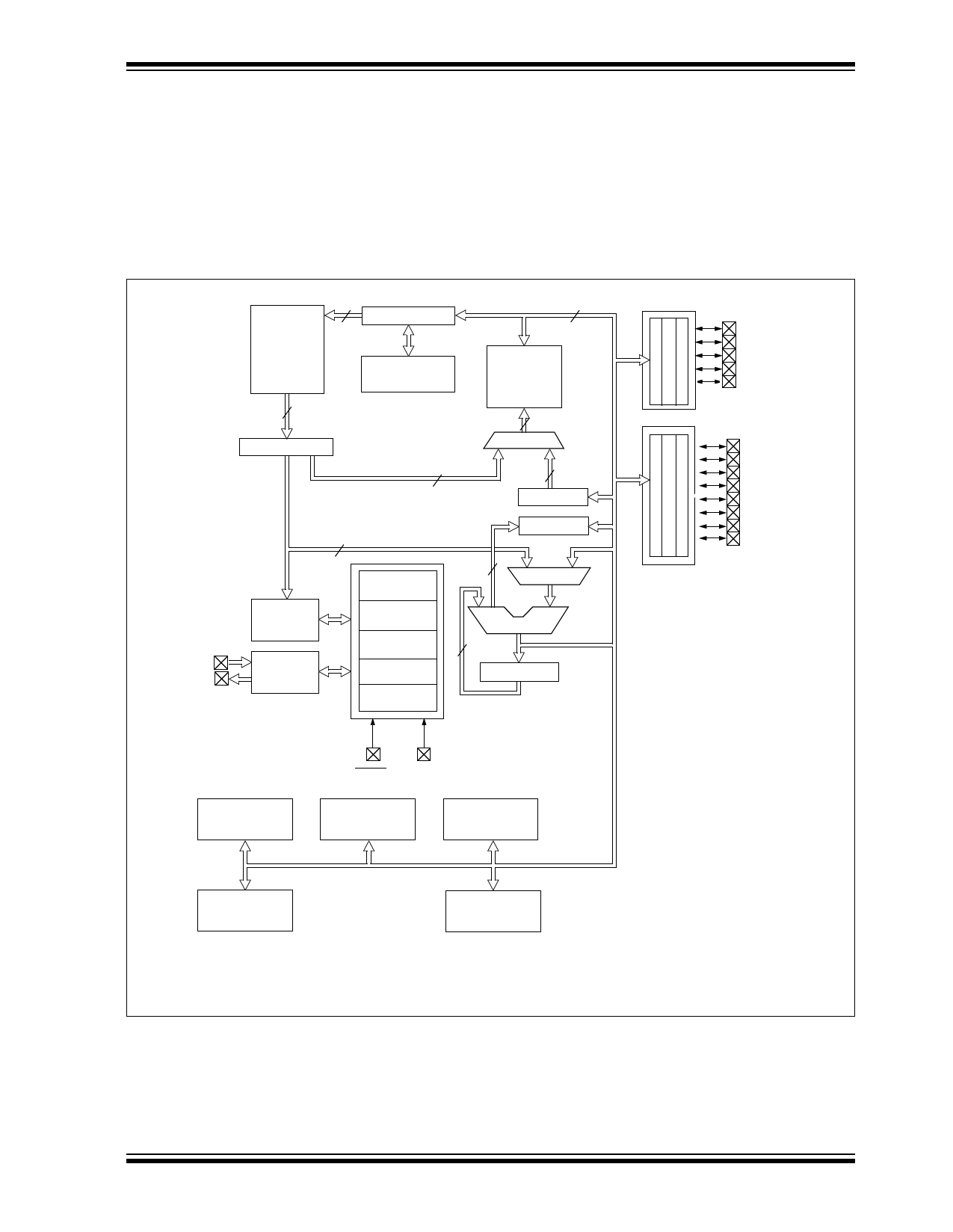
Figure 1-1 is the block diagram for both devices. The
pinouts are listed in Table 1-1.
FIGURE 1-1: PIC16C712/716 BLOCK DIAGRAM
EPROM
1K X 14
or
2K x 14
Program
Memory
Program
Bus
14
Instruction reg
13
Program Counter
Data Bus
8
8 Level Stack
(13-bit)
RAM
128 x 8
File
Registers
RAM Addr(1)
9
Addr MUX
Direct Addr 7
Indirect
8 Addr
FSR reg
STATUS reg
8
OSC1/CLKIN
OSC2/CLKOUT
Instruction
Decode &
Control
Timing
Generation
Power-up
Timer
Oscillator
Start-up Timer
Power-on
Reset
Watchdog
Timer
Brown-out
Reset
3
MUX
ALU
8
W reg
PORTA
PORTB
RA0/AN0
RA1/AN1
RA2/AN2
RA3/AN3/VREF
RA4/T0CKI
RB0/INT
RB1/T1OSO/T1CKI
RB2/T1OSI
RB3/CCP1
RB4
RB5
RB6
RB7
Timer0
MCLR VDD, VSS
Timer1
Timer2
CCP1
A/D
Note 1: Higher order bits are from the STATUS register.
© 1999 Microchip Technology Inc.
Preliminary
DS41106A-page 5
Share Link: 