R5F212C7SDFP 查看數據表(PDF) - Renesas Electronics
零件编号
产品描述 (功能)
比赛名单
R5F212C7SDFP Datasheet PDF : 58 Pages
| |||
R8C/2C Group, R8C/2D Group
4. Special Function Registers (SFRs)
4. Special Function Registers (SFRs)
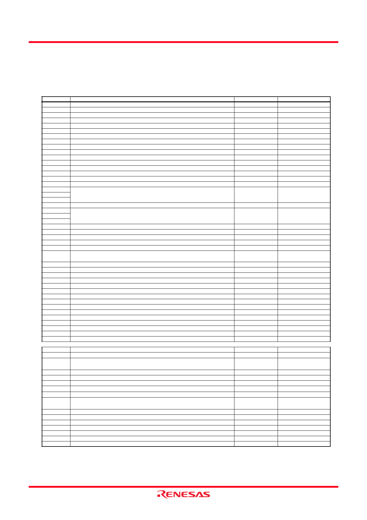
An SFR (special function register) is a control register for a peripheral function. Tables 4.1 to 4.12 list the special
function registers.
Table 4.1 SFR Information (1)(1)
Address
0000h
0001h
0002h
0003h
0004h
0005h
0006h
0007h
0008h
0009h
000Ah
000Bh
000Ch
000Dh
000Eh
000Fh
0010h
0011h
0012h
0013h
0014h
0015h
0016h
0017h
0018h
0019h
001Ah
001Bh
001Ch
Register
Processor Mode Register 0
Processor Mode Register 1
System Clock Control Register 0
System Clock Control Register 1
Module Operation Enable Register
Protect Register
Oscillation Stop Detection Register
Watchdog Timer Reset Register
Watchdog Timer Start Register
Watchdog Timer Control Register
Address Match Interrupt Register 0
Address Match Interrupt Enable Register
Address Match Interrupt Register 1
Count Source Protection Mode Register
001Dh
001Eh
001Fh
0020h
0021h
0022h
0023h
0024h
0025h
0026h
0027h
0028h
0029h
002Ah
002Bh
High-Speed On-Chip Oscillator Control Register 0
High-Speed On-Chip Oscillator Control Register 1
High-Speed On-Chip Oscillator Control Register 2
Clock Prescaler Reset Flag
High-Speed On-Chip Oscillator Control Register 6
Symbol
After reset
PM0
PM1
CM0
CM1
MSTCR
PRCR
OCD
WDTR
WDTS
WDC
RMAD0
AIER
RMAD1
00h
00h
01101000b
00100000b
00h
00h
00000100b
XXh
XXh
00X11111b
00h
00h
00h
00h
00h
00h
00h
CSPR
00h
10000000b(6)
FRA0
FRA1
FRA2
CPSRF
FRA6
00h
When shipping
00h
00h
When Shipping
0030h
0031h
0032h
0033h
0034h
0035h
0036h
0037h
0038h
0039h
003Ah
003Bh
003Ch
003Dh
003Eh
003Fh
Voltage Detection Register 1(2)
Voltage Detection Register 2(2)
Voltage Monitor 1 Circuit Control Register(5)
Voltage Monitor 2 Circuit Control Register(5)
Voltage Monitor 0 Circuit Control Register(2)
VCA1
VCA2
VW1C
VW2C
VW0C
00001000b
00h(3)
00100000b(4)
00001000b
00h
0000X000b(3)
0100X001b(4)
X: Undefined
NOTES:
1. The blank regions are reserved. Do not access locations in these regions.
2. Software reset, watchdog timer reset, voltage monitor 1 reset, or voltage monitor 2 reset do not affect this register.
3. The LVD0ON bit in the OFS register is set to 1 and hardware reset.
4. Power-on reset, voltage monitor 0 reset, or the LVD0ON bit in the OFS register is set to 0 and hardware reset.
5. Software reset, watchdog timer reset, voltage monitor 1 reset, or voltage monitor 2 reset do not affect b2 and b3.
6. The CSPROINI bit in the OFS register is set to 0.
Rev.1.00 Feb 09, 2007 Page 19 of 55
REJ03B0183-0100
Share Link: 