RD74LVC1G240 查看數據表(PDF) - Renesas Electronics
零件编号
产品描述 (功能)
比赛名单
RD74LVC1G240 Datasheet PDF : 8 Pages
| |||
RD74LVC1G240
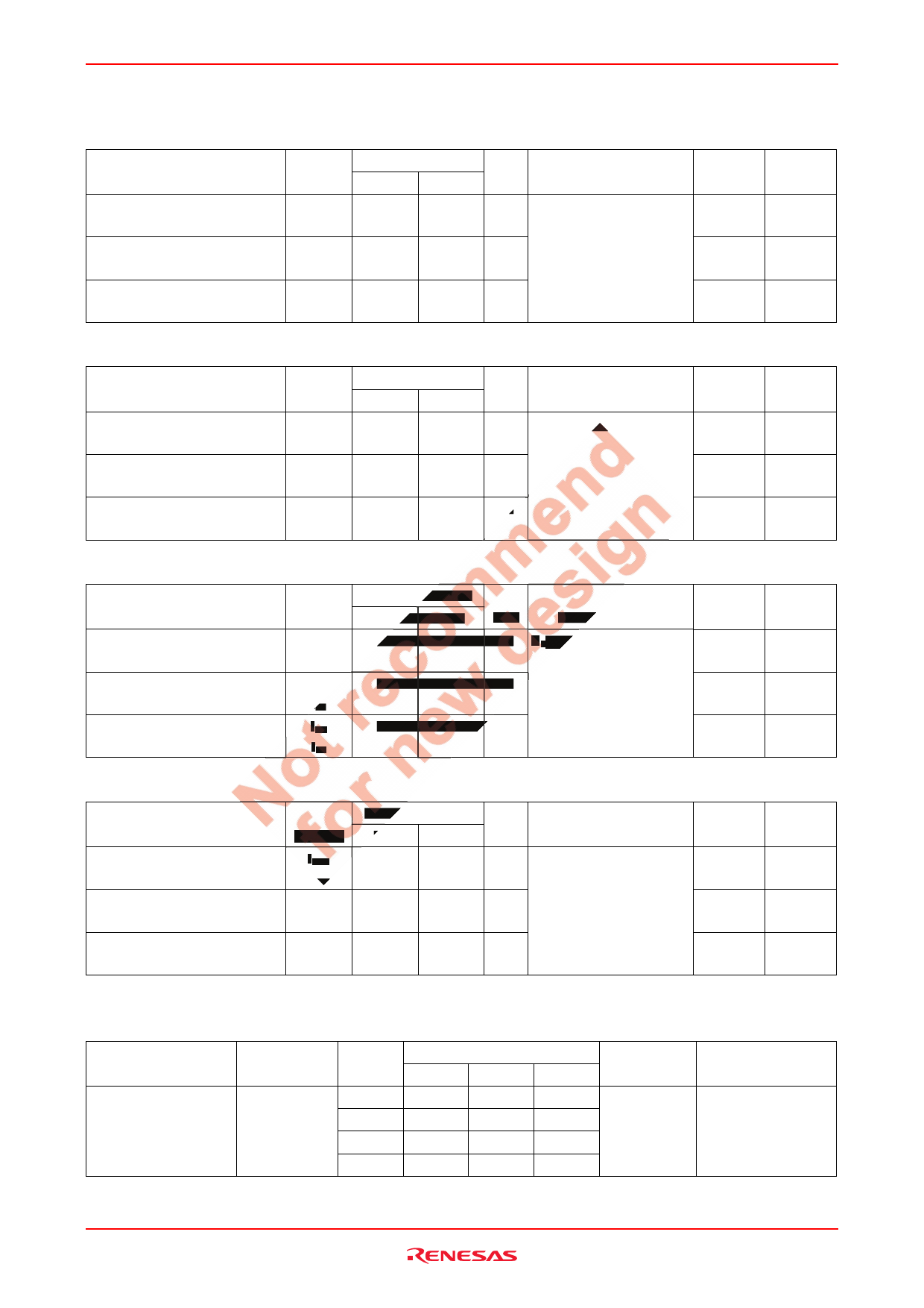
Switching Characteristics
Item
Propagation delay time
Output enable time
Output disable time
Symbol
tPLH
tPHL
tZH
tZL
tHZ
tLZ
Ta = –40 to 85°C
Min
Max
3.0
8.0
3.8
9.4
2.1
9.4
Unit
Test Conditions
ns CL = 30 pF, RL = 1.0 kΩ
ns
ns
VCC = 1.8±0.15 V
FROM
TO
(Input) (Output)
A
Y
OE
Y
OE
Y
Item
Propagation delay time
Output enable time
Output disable time
Symbol
tPLH
tPHL
tZH
tZL
tHZ
tLZ
Ta = –40 to 85°C
Min
Max
1.4
5.5
2.1
6.5
1.0
4.9
Unit
Test Conditions
ns CL = 30 pF, RL = 500 Ω
ns
ns
VCC = 2.5±0.2 V
FROM
TO
(Input) (Output)
A
Y
OE
Y
OE
Y
Item
Propagation delay time
Output enable time
Output disable time
Symbol
tPLH
tPHL
tZH
tZL
tHZ
tLZ
Ta = –40 to 85°C
Min
Max
1.1
4.5
1.4
5.4
1.4
5.2
Unit
Test Conditions
ns CL = 50 pF, RL = 500 Ω
ns
ns
VCC = 3.3±0.3 V
FROM
TO
(Input) (Output)
A
Y
OE
Y
OE
Y
Item
Propagation delay time
Output enable time
Output disable time
Symbol
tPLH
tPHL
tZH
tZL
tHZ
tLZ
Ta = –40 to 85°C
Min
Max
1.0
4.0
1.1
5.2
1.0
4.1
Unit
Test Conditions
ns CL = 50 pF, RL = 500 Ω
ns
ns
VCC = 5.0±0.5 V
FROM
TO
(Input) (Output)
A
Y
OE
Y
OE
Y
Operating Characteristics
Item
Power dissipation
capacitance
Symbol
CPD
VCC (V)
1.8
2.5
3.3
5.0
Ta = 25°C
Min
Typ
Max
—
19
—
—
19
—
—
20
—
—
22
—
Unit
Test Conditions
pF
f = 10 MHz
Rev.1.00 Apr 13, 2006 page 5 of 7
Share Link: 