RT9248 查看數據表(PDF) - Richtek Technology
零件编号
产品描述 (功能)
比赛名单
RT9248 Datasheet PDF : 14 Pages
| |||
RT9248
Preliminary
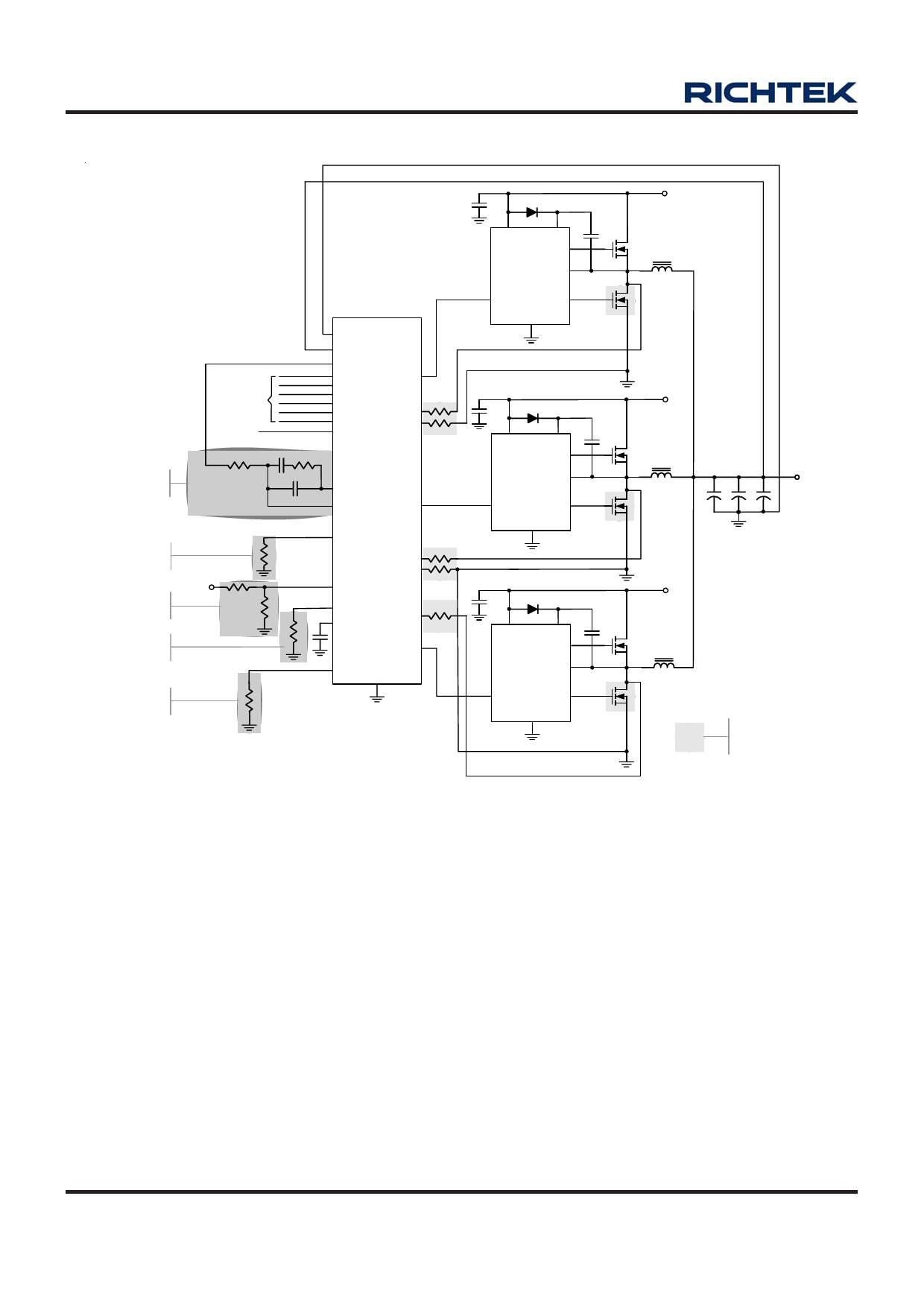
3-Phase Converter and Components Function Grouping
12V
VCC
BST
DRVH
SGND
VSEN
VDIF
PWM1
SW
RT9603
IN
DRVL
PGND
VID
PGOOD
12V
ISP1
ISN1
VCC
BST
Compensation
& Offset
RT9248
COMP
DRVH
SW
RT9603
FB
PWM2
IN
DRVL
PGND
ADJ
Droop Setting
ISP2
ISN23
12V
Driver Power
UVLO
DAC Offset
Voltage Setting
DVD
12V
VOSS
SS
ISP3
PWM3
VCC
BST
DRVH
OCP Setting
IMAX
GND
SW
RT9603
IN
DRVL
PGND
VCORE
Current Sense
Components
Design Procedure Suggestion
Voltage Loop Setting
a. Output filter pole and zero (Inductor, output capacitor
value & ESR).
b. Error amplifier compensation & sawtooth wave amp-
litude (compensation network).
c. Kelvin sense for VCORE.
Current Loop Setting
a. GM amplifier S/H current (current sense component
R , ISPx & ISNx pin external resistor value,
DS(ON)
keep ISPx current < 60μA at full load condition for
better load line linearity).
b. Over-current protection trip point (IMAX pin resistor,
keep ISPx current < 90μA at OCP condition for
precision issue).
www.richtek.com
10
VRM Load Line Setting
a. Droop amplitude (ADJ pin resistor).
b. No load offset (additional resistor in compensation
network).
c. DAC offset voltage setting (VOSS pin & compen-
sation network resistor).
Power Sequence & SS
DVD pin external resistor and SS pin capacitor.
PCB Layout
a. Kelvin sense for current sense GM amplifier input.
b. Refer to layout guide for other item.
DS9248-05 March 2007
Share Link: 