FBL2031BB 查看數據表(PDF) - Philips Electronics
零件编号
产品描述 (功能)
比赛名单
FBL2031BB Datasheet PDF : 16 Pages
| |||
Philips Semiconductors
9-bit BTL 3.3V latched/registered/pass-thru
Futurebus+ transceiver
Product specification
FBL2031
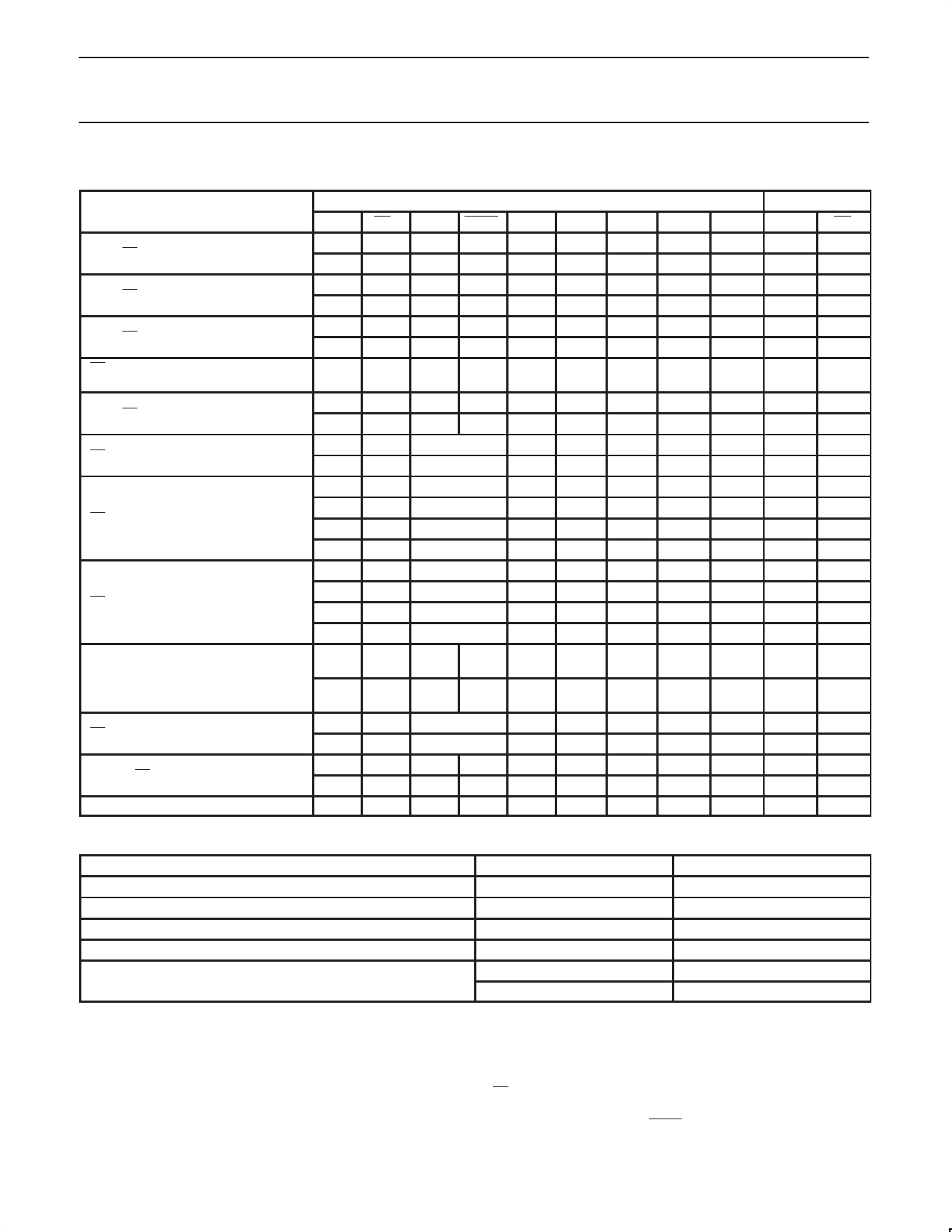
FUNCTION TABLE
MODE
An to Bn thru mode
An to Bn transparent latch
An to Bn latch and read
Bn outputs latched and read
(preconditioned latch)
An to Bn register
Bn to An thru mode
Bn to An transparent latch
Bn to An latch and read
An outputs latched and read
(preconditioned latch)
Bn to An register
Disable Bn outputs
Disable An outputs
INPUTS
OUTPUTS
An Bn* OEB0 OEB1 OEA LCAB LCBA SEL0 SEL1 An
Bn
L
—
H
L
L
X
X
H
L
input H**
H
—
H
L
L
X
X
H
L
input
L
L
—
H
L
L
L
X
L
L
input H**
H
—
H
L
L
L
X
L
L
input
L
l
—
H
L
L
↑
X
L
L
input H**
h
—
H
L
L
↑
X
L
L
input
L
X
—
H
L
X
H
X
L
L
X
latched
data
l
—
H
L
L
↑
X
X
H
input H**
h
—
H
L
L
↑
X
X
H
input
L
—
L
Disable
H
X
X
H
L
H
input
—
H
Disable
H
X
X
H
L
L
input
—
L
Disable
H
X
L
L
L
H
input
—
H
Disable
H
X
L
L
L
L
input
—
L
Disable
H
X
L
H
H
H
input
—
H
Disable
H
X
L
H
H
L
input
—
l
Disable
H
X
↑
L
L
H
input
—
h
Disable
H
X
↑
L
L
L
input
—
l
Disable
H
X
↑
H
H
H
input
—
h
Disable
H
X
↑
H
H
L
input
—
X
X
X
H
X
H
L
L
latched
data
X
—
X
X
X
H
X
H
H
H
latched
data
X
—
l
Disable
H
X
↑
L
H
H
input
—
h
Disable
H
X
↑
L
H
L
input
X
X
L
X
X
X
X
X
X
X
H**
X
X
X
H
X
X
X
X
X
X
H**
X
X
X
X
L
X
X
X
X
Z
X
FUNCTION SELECT TABLE
MODE SELECTED
Thru mode
Register mode (An to Bn)
Latch mode (An to Bn)
Register mode (Bn to An)
Latch mode (Bn to An)
NOTES:
H = High voltage level
L = Low voltage level
l = Low voltage level one set-up time prior to the Low-to-High
LCXX transition
h = High voltage level one set-up time prior to the Low-to-High
LCXX transition
X = Don’t care
SEL0
H
X
L
L
L
H
SEL1
L
H
L
H
L
H
Z = High-impedance (OFF) state
— = Input not externally driven
↑ = Low-to-High transition
H** = Goes to level of pull-up voltage
Bn* = Precaution should be taken to ensure B inputs do not float.
If they do, they are equal to Low state.
Disable = OEB0 is Low or OEB1 is High.
2000 Apr 18
5
Share Link: 