FBL2031BB 查看數據表(PDF) - Philips Electronics
零件编号
产品描述 (功能)
比赛名单
FBL2031BB Datasheet PDF : 16 Pages
| |||
Philips Semiconductors
9-bit BTL 3.3V latched/registered/pass-thru
Futurebus+ transceiver
Product specification
FBL2031
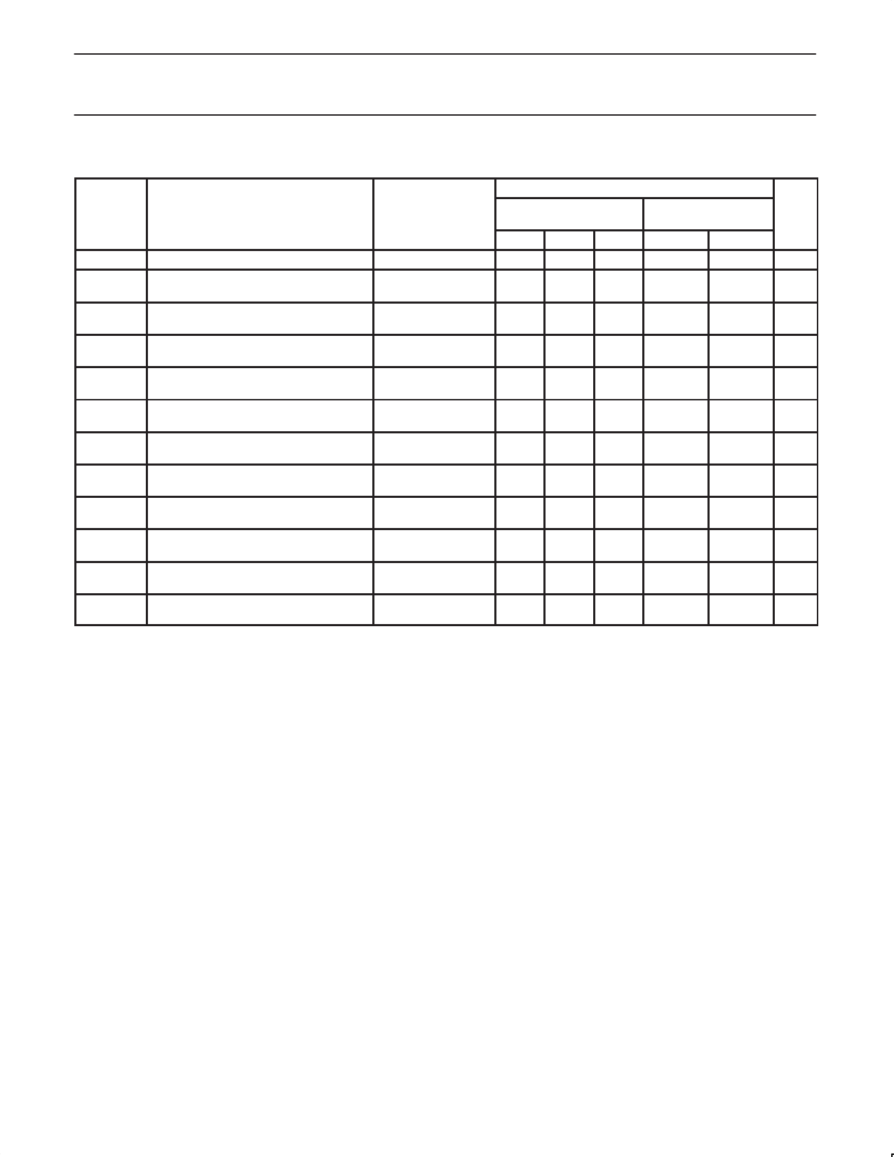
AC ELECTRICAL CHARACTERISTICS
B TO A SPECIFICATIONS
SYMBOL
PARAMETER
TEST
CONDITION
Tamb = +25°C,
VCC = 3.3V,
MIN TYP MAX
Tamb = –40 to +85°C,
VCC = 3.3V±10%,
MIN
MAX
UNIT
fMAX
Maximum clock frequency
Waveform 4
120 150
MHz
tPLH
Propagation delay (thru mode)
tPHL
Bn to An
Waveform 1, 2
2.8
4.3
5.9
3.0
4.5
6.0
2.2
2.6
6.8
7.3
ns
tPLH
Propagation delay (transparent latch)
tPHL
Bn to An
Waveform 1, 2
2.8
4.9
7.0
3.4
5.0
6.6
1.8
2.8
8.4
7.8
ns
tPLH
Propagation delay
tPHL
LCBA to An (latch)
Waveform 1, 2
7.7 10.2 13.0
6.1
7.5 10.1 12.9
6.1
15.6
15.4
ns
tPLH
Propagation delay
tPHL
LCBA to An (register)
Waveform 1, 2
2.7
4.2
5.7
3.0
4.5
6.1
2.1
2.4
6.7
6.9
ns
tPLH
Propagation delay
tPHL
SEL0 or SEL1 to An (inverting)
Waveform 1, 2
2.9
5.8
9.1
2.2
1.9
5.8 10.4
1.2
10.5
11.6
ns
tPLH
Propagation delay
tPHL
SEL0 or SEL1 to An (non-inverting)
Waveform 1, 2
2.0
5.9 10.3
1.4
2.8
5.6
8.8
2.2
12.3
10.0
ns
tPZH
Output enable time from High or Low
tPHZ
OEA to An
Waveform 5, 6
3.0
4.4
5.7
4.0
5.6
7.3
2.6
3.2
6.6
8.3
ns
tPZL
Output disable time to High or Low
tPLZ
OEA to An
Waveform 5, 6
2.6
4.0
5.4
1.4
2.6
3.7
2.1
1.0
6.0
4.4
ns
tTLH
Output transition time, An Port
tTHL
10% to 90%, 90% to 10%
Test Circuit and
Waveforms
0.2
0.1
2.0
1.2
ns
tSK(o)
Output to output skew for multiple
channels1
Waveform 3
0.5
1.0
1.5
ns
tSK(p)
Pulse skew2
tPHL – tPLH MAX
Waveform 2
0.5
1.0
1.5
ns
NOTES:
1. tPNactual – tPMactual for any data input to output path compared to any other data input to output path where N and M are either LH or HL.
Skew times are valid only under same test conditions (temperature, VCC, loading, etc.). tSK (0) compares tPLH on a given path to tPLH on
any other path or compares tPHL on a given path to tPHL on any other path.
2. tSK(p) is used to quantify duty cycle characteristics. In essence it compares the input signal duty cycle to the corresponding output signal
duty cycle (50MHz input frequency and 50% duty cycle, tested on data paths only).
2000 Apr 18
9
Share Link: 