SAF-XC835MT-2FGI 查看數據表(PDF) - Infineon Technologies
零件编号
产品描述 (功能)
比赛名单
SAF-XC835MT-2FGI Datasheet PDF : 56 Pages
| |||
XC835/836
General Device Information
2.5
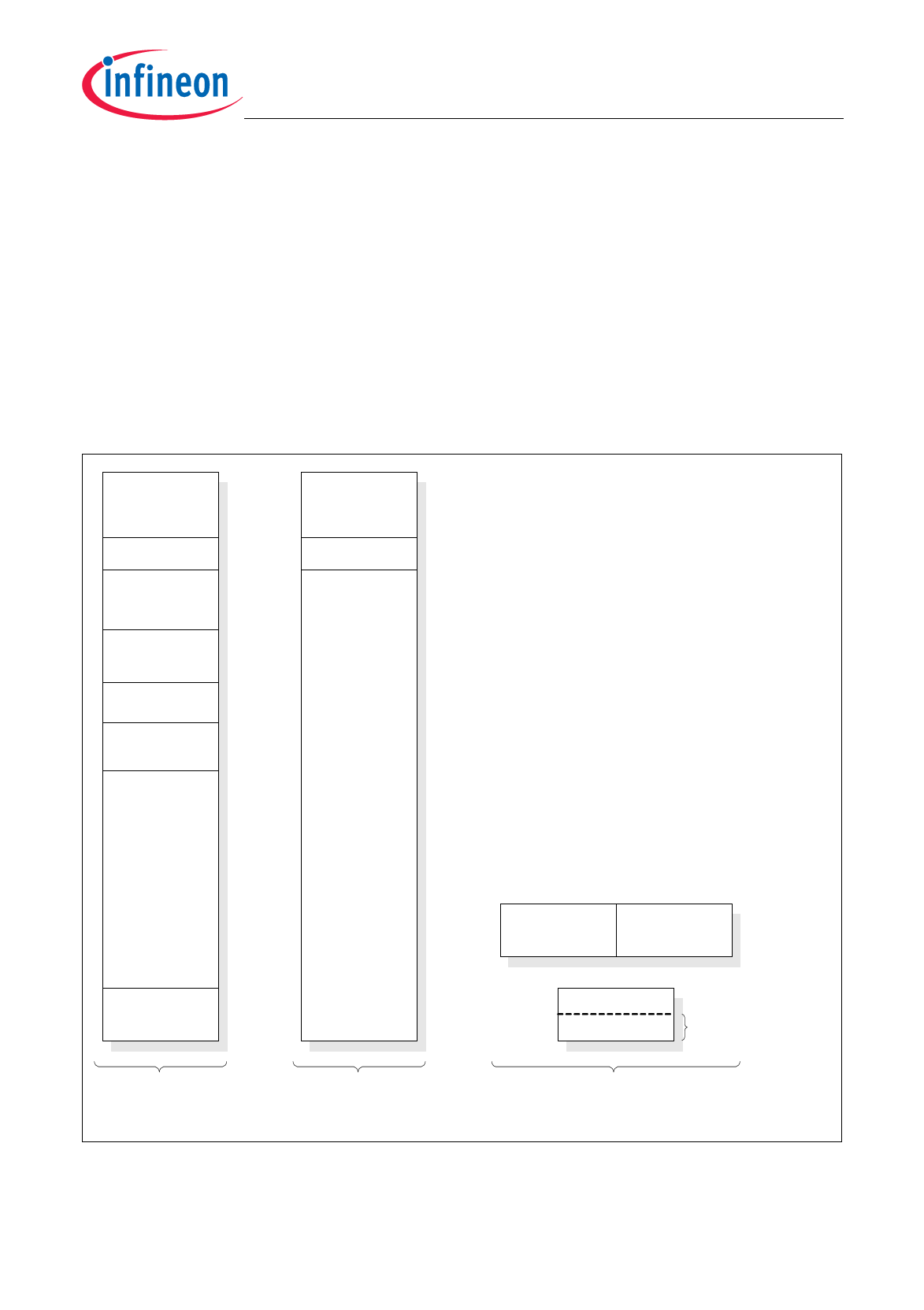
Memory Organization
The XC835/836 CPU operates in the following five address spaces:
• 8 Kbytes of Boot ROM, Library ROM and User routines
• 256 bytes of internal RAM
• 256 bytes of XRAM
(XRAM can be read/written as program memory or external data memory)
• A 128-byte Special Function Register area
• 4/8 Kbytes of Flash
Figure 6 illustrates the memory address spaces of the 4 Kbyte Flash devices. Figure 7
illustrates the memory address spaces of the 8 Kbyte Flash devices.
FFFF H
FFFF H
XRAM
256 Bytes
F100H
F000H
XRAM
256 Bytes
F100H
F000H
Boot ROM
8 KBytes
Flash Bank 0
4 KBytes 1)
E000H
C000H
B000H
A000H
Flash Bank 0
4 KBytes
1000H
0000H
0000H
Indirect
Address
Internal RAM
Direct
Address
FFH
Special Function
Registers
80H
7FH
Internal RAM
40H
00H
In Debug Mode, this 64-byte address area
is replaced by a 64-byte Monitor RAM.
Code Space
External Data Space
1) Physically one 4-Kbyte Flash bank, mapped to both address range .
Internal Data Space
Memory Map User Mode
Figure 6 Memory Map of XC835/836 with 4 Kbytes of Flash memory
Data Sheet
18
V1.2, 2011-03
Share Link: 