UT62L64CPC-70 查看數據表(PDF) - Utron Technology Inc
零件编号
产品描述 (功能)
比赛名单
UT62L64CPC-70 Datasheet PDF : 12 Pages
| |||
UTRON
Rev. 1.4
FEATURES
Access time : 35/70ns (max.)
Low power consumption :
Operating : 40/30 mA (typ.)
CMOS Standby : 0.3mA (typ.) normal
2 µA (typ.) L-version
1 µA (typ.) LL-version
Single 4.5V~5.5V power supply
Operating temperature :
Commercial : 0℃~70℃
Extended : -20℃~85℃
All inputs and outputs TTL compatible
Fully static operation
Three state outputs
Data retention voltage : 2V (min.)
Package : 28-pin 600 mil PDIP
28-pin 330 mil SOP
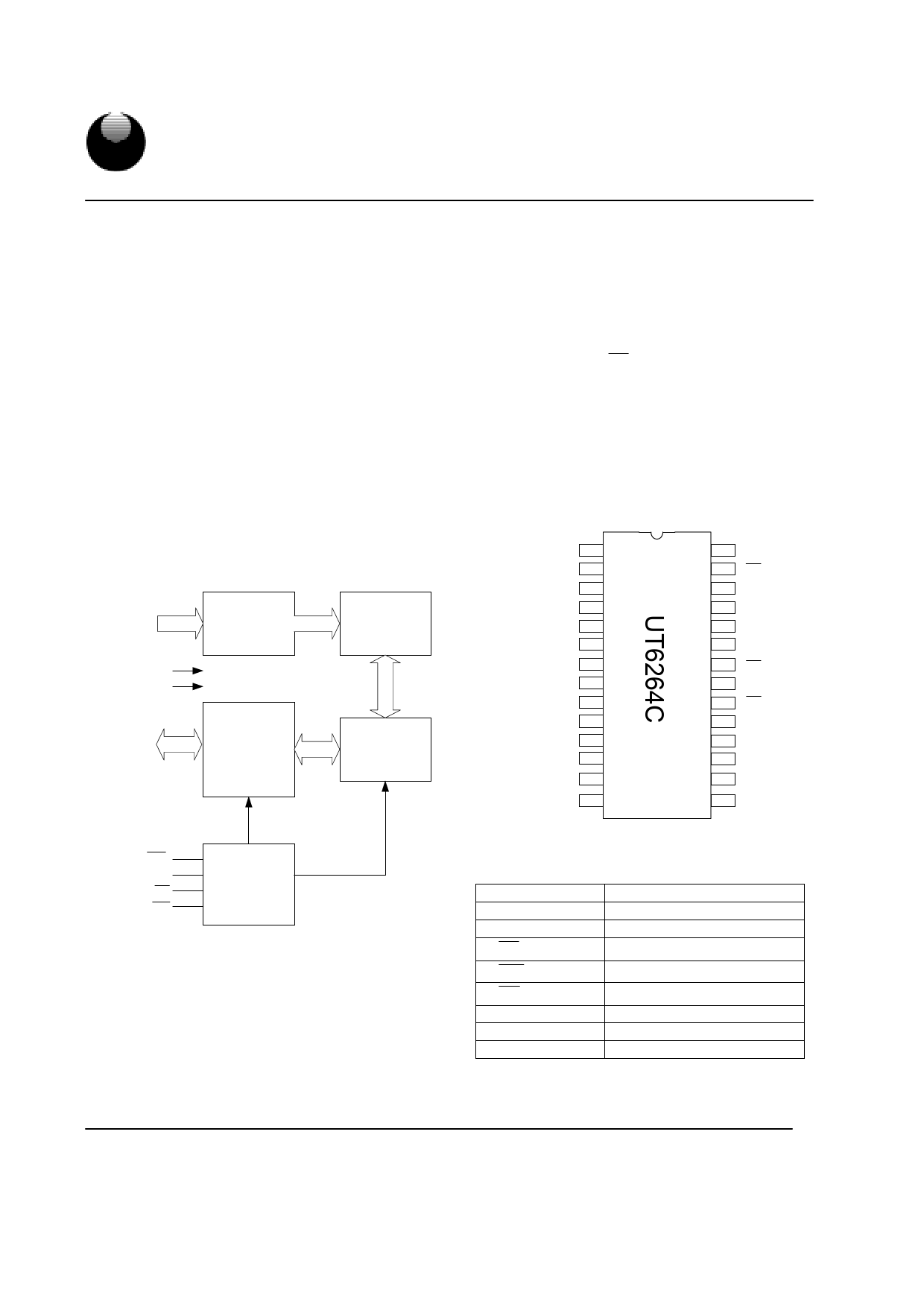
FUNCTIONAL BLOCK DIAGRAM
A0-A12
Vcc
Vss
DECODER
8K X 8
MEMORY
ARRAY
I/O1-I/O8
I/O DATA
CIRCUIT
COLUMN I/O
CE
CE2
OE
WE
CONTROL
CIRCUIT
UT6264C
8K X 8 BIT LOW POWER CMOS SRAM
GENERAL DESCRIPTION
The UT6264C is a 65,536-bit low power CMOS static
random access memory organized as 8,192 words by
8 bits. It is fabricated using high performance, high
reliability CMOS technology.
Easy memory expansion is provided by using two
chip enable input.( CE ,CE2) ,and supports low data
retention voltage for battery back-up operation with
low data retention current.
The UT6264C operates from a single 4.5V~5.5V
power supply and all inputs and outputs are fully TTL
compatible.
PIN CONFIGURATION
NC
1
A12
2
A7
3
A6
4
A5
5
A4
6
A3
7
A2
8
A1
9
A0
10
I/O1
11
I/O2
12
I/O3
13
Vss
14
28
Vcc
27
WE
26
CE2
25
A8
24
A9
23
A11
22
OE
21
A10
20
CE
19
I/O8
18
I/O7
17
I/O6
16
I/O5
15
I/O4
PDIP/SOP
PIN DESCRIPTION
SYMBOL
A0 - A12
I/O1 - I/O8
CE ,CE2
WE
OE
VCC
VSS
NC
DESCRIPTION
Address Inputs
Data Inputs/Outputs
Chip Enable Inputs
Write Enable Input
Output Enable Input
Power Supply
Ground
No connection
UTRON TECHNOLOGY INC.
1F, No. 11, R&D Rd. II, Science-Based Industrial Park, Hsinchu, Taiwan, R. O. C.
TEL: 886-3-5777882 FAX: 886-3-5777919
2
P80028
Share Link: 