ADG728 查看數據表(PDF) - Analog Devices
零件编号
产品描述 (功能)
比赛名单
ADG728 Datasheet PDF : 13 Pages
| |||
ADG728/ADG729
PIN FUNCTION DESCRIPTIONS
ADG728
1
2
3
4, 5, 6, 7
8
9, 10, 11, 12
13
14
15
16
ADG729
1
Mnemonic
SCL
RESET
3
SDA
4, 5, 6, 7
8, 9
10, 11, 12, 13
14
15
2
16
Sxx
Dx
Sxx
VDD
GND
A1
A0
Function
Serial Clock Line. This is used in conjunction with the SDA line to clock data into
the 8-bit input shift register. Clock rates of up to 400 kbit/s can be accommodated
with this 2-wire serial interface.
Active low control input that clears the input register and turns all switches to the
OFF condition.
Serial Data Line. This is used in conjunction with the SCL line to clock data into
the 8-bit input shift register during the write cycle and used to read back 1 byte of
data during the read cycle. It is a bidirectional open-drain data line which should be
pulled to the supply with an external pull-up resistor.
Source. May be an input or output.
Drain. May be an input or output.
Source. May be an input or output.
Power Supply Input. These parts can be operated from a supply of 2.7 V to 5.5 V.
Ground Reference.
Address Input. Sets the second least significant bit of the 7-bit slave address.
Address Input. Sets the least significant bit of the 7-bit slave address.
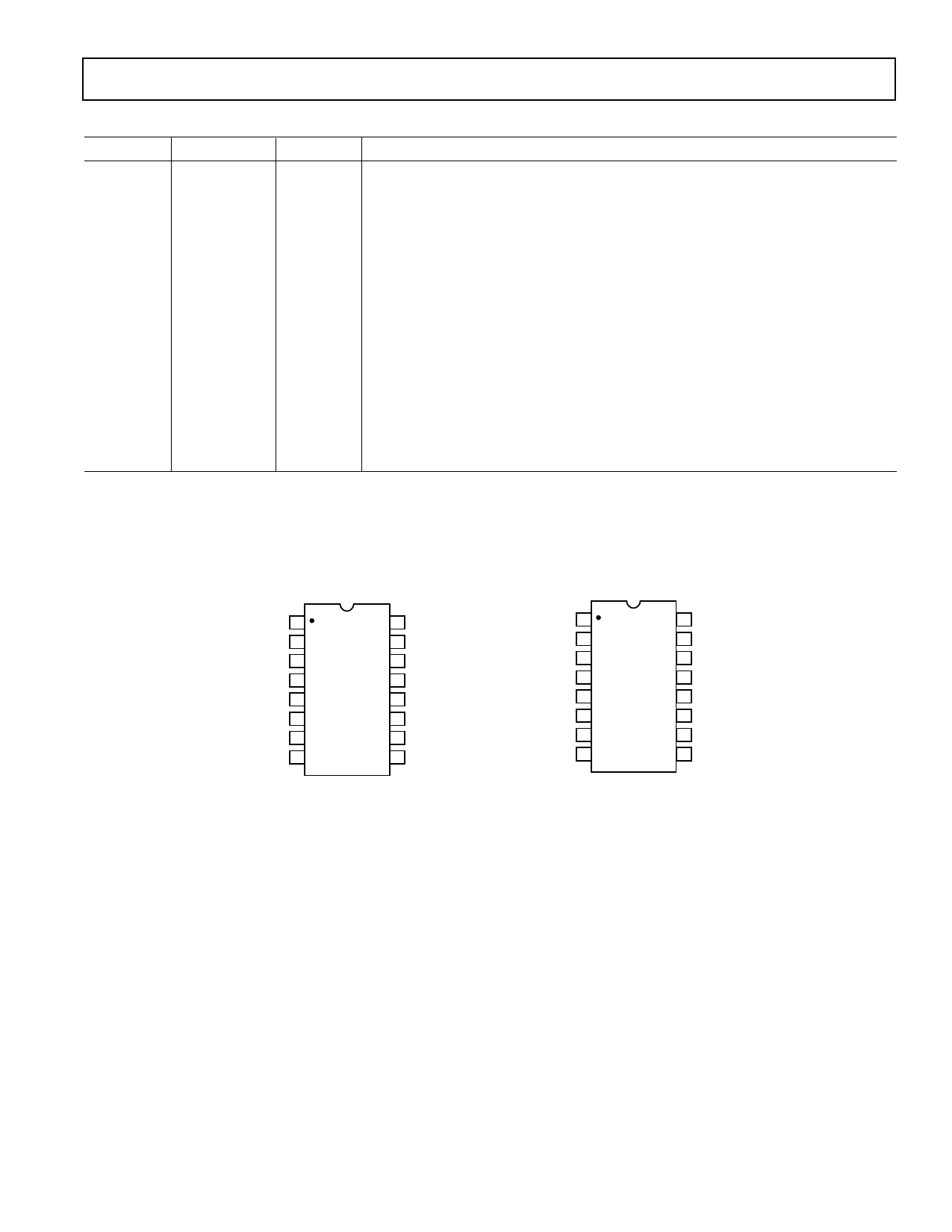
PIN CONFIGURATIONS
ADG728
ADG729
SCL 1
RESET 2
SDA 3
S1 4
S2 5
S3 6
S4 7
D8
ADG728
TOP VIEW
(Not to Scale)
16 A0
15 A1
14 GND
13 VDD
12 S5
11 S6
10 S7
9 S8
SCL 1
A1 2
SDA 3
S1A 4
S2A 5
S3A 6
S4A 7
DA 8
ADG729
TOP VIEW
(Not to Scale)
16 A0
15 GND
14 VDD
13 S1B
12 S2B
11 S3B
10 S4B
9 DB
REV. C
–5–
Share Link: 