ADG714(Rev0) 查看數據表(PDF) - Analog Devices
零件编号
产品描述 (功能)
比赛名单
ADG714 Datasheet PDF : 16 Pages
| |||
ADG714/ADG715
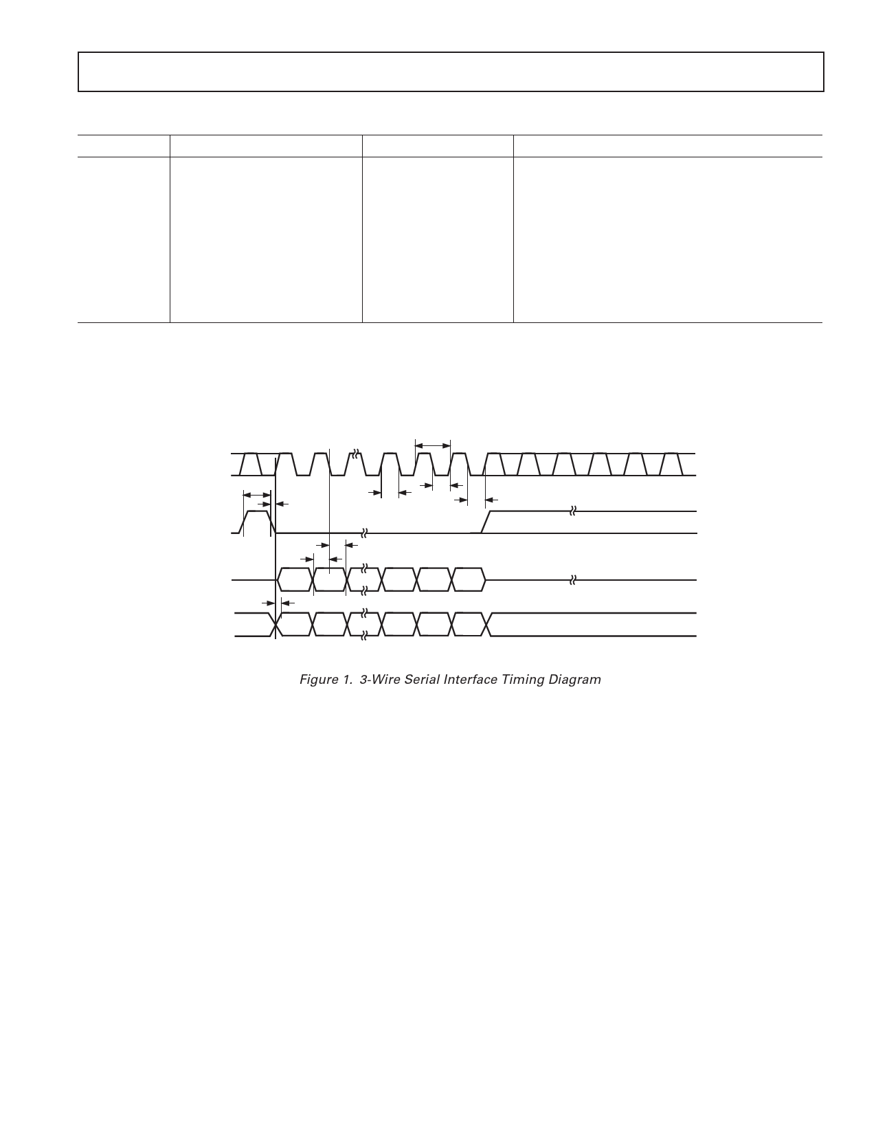
ADG714 TIMING CHARACTERISTICS1, 2 (VDD = 2.7 V to 5.5 V. All specifications –40؇C to +85؇C unless otherwise noted.)
Parameter
Limit at TMIN, TMAX
Unit
Conditions/Comments
fSCLK
30
t1
33
t2
13
t3
13
t4
0
t5
5
t6
4.5
t7
0
t8
33
t93
20
MHz max
ns min
ns min
ns min
ns min
ns min
ns min
ns min
ns min
ns min
SCLK Cycle Frequency
SCLK Cycle Time
SCLK High Time
SCLK Low Time
SYNC to SCLK Rising Edge Setup Time
Data Setup Time
Data Hold Time
SCLK Falling Edge to SYNC Rising Edge
Minimum SYNC High Time
SCLK Rising Edge to DOUT Valid
NOTES
1See Figure 1.
2All input signals are specified with tr = tf = 5 ns (10% to 90% of VDD) and timed from a voltage level of (VIL + VIH)/2.
3CL = 20 pF, RL = 1 kΩ.
Specifications subject to change without notice.
t1
SCLK
SYNC
DIN
DOUT
t8
t4
t6
t5
DB7
t9
DB71
DB61
t2
t3
t7
DB0
DB21 DB11 DB01
NOTE
1DATA FROM PREVIOUS WRITE CYCLE
Figure 1. 3-Wire Serial Interface Timing Diagram
REV. 0
–5–
Share Link: 