LC11014-241 查看數據表(PDF) - SANYO -> Panasonic
零件编号
产品描述 (功能)
比赛名单
LC11014-241 Datasheet PDF : 13 Pages
| |||
LC11014-241
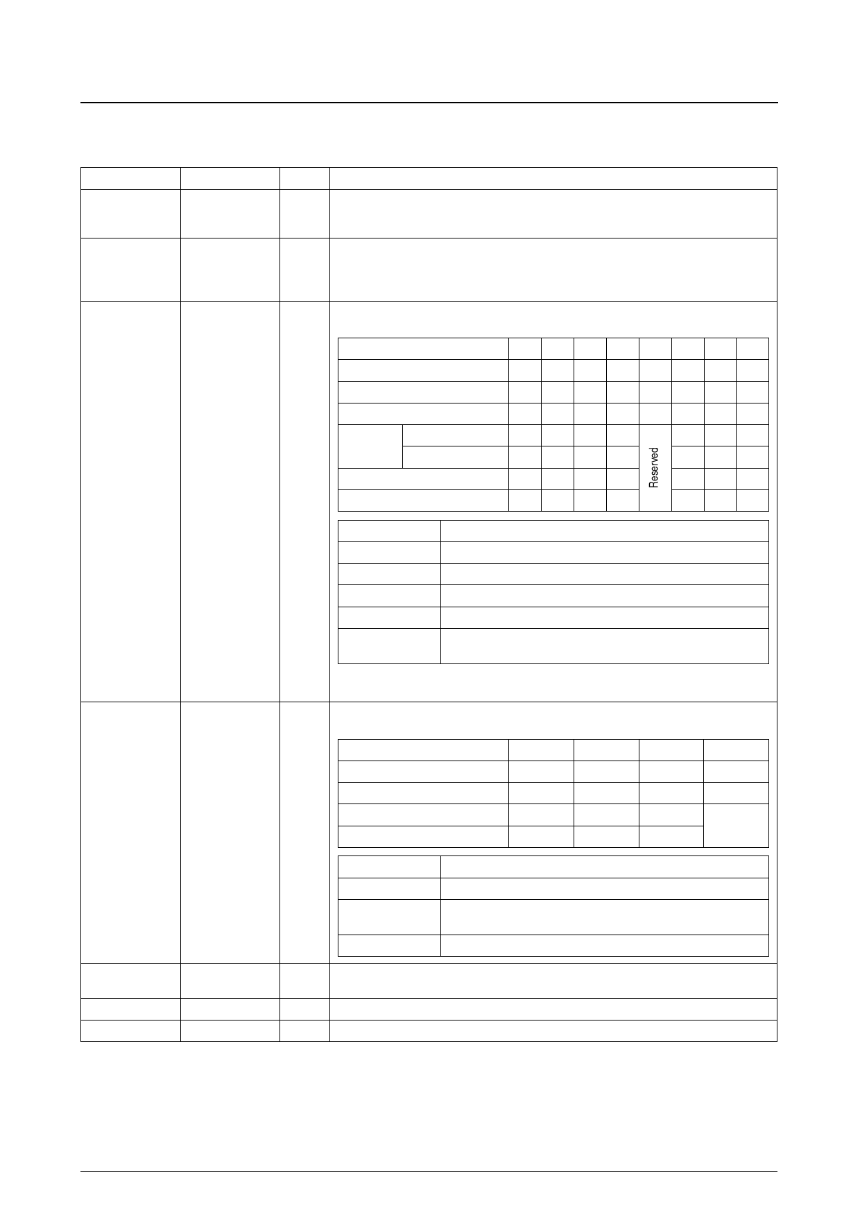
Pin Functions
Symbol
VDD
VSS
GSPMD [0:2]
IOMD [0:1]
VMD
SCLK
DSIFT
Pin No.
9, 18, 29, 37, 43, 49,
54, 60, 68, 73, 90,
109, 126, 144
1, 12, 19, 24, 30, 36,
42, 48, 55, 61, 65,
67, 72, 82, 91, 100,
108, 118, 127, 135
74 to 76
2, 3
77
81
143
I/O
– Supply voltage (+3.3V)
Function
– Ground (0V)
Mode selection signals [0 to 2] for the gray-scale mode. The setting process for the mode selection lines
is described below. GSPMD0 is the LSB and GSPMD2 is the MSB.
Gray-scale mode
01234567
GSPMD0
LHLHLHLH
GSPMD1
L LHHL LHH
GSPMD2
L L L LHHHH
Intra-frame processing Yes Yes Yes Yes
Processing
Inter-frame processing Yes Yes Yes Yes
Yes Yes Yes
No No No
Number of valid input bits
8888
888
I
Number of output bits
3456
456
Gray-scale mode
LCD module
0
Operating mode for TFT LCD modules with 3-bit source driver
1
Operating mode for TFT LCD modules with 4-bit source driver
2, 6
Operating mode for TFT LCD modules with 5-bit source driver
3, 7
Operating mode for TFT LCD modules with 6-bit source driver
5
Operating mode for TFT LCD modules with 3-bit source driver that perform
FRC or other inter-frame processing
Do not use gray-scale modes 0 to 3 with TFT LCD modules that perform FRC or other inter-frame
processing.
Input/output mode select pins. The input/output mode selection lines are described below. IOMD0 is the
LSB and IOMD1 is the MSB.
Input/output mode
0
1
2
3
IOMD0
L
H
L
H
IOMD1
L
L
H
H
Input
Parallel
Serial
Serial
I
Output
Parallel
Parallel
Serial
Reserved
Input/output mode
0
1
2
LCD module
XGA-compatible 2-pixel parallel input interface TFT LCD panels
2-pixel parallel input interface TFT LCD panels (serial input is converted to
parallel internally)
Serial input interface VGA and SVGA TFT LCD panels
I
Gray-scale processing algorithm select pin. The LC11011-141 algorithm is selected when high. Normal
mode is selected when low or open.
I Clock signal input. Data is processed according to this clock signal.
I
In input/output mode 1, data is shifted out on both ×D0 and ×D1 when high.
No. 5578—4/13
Share Link: 