UPD16835 查看數據表(PDF) - NEC => Renesas Technology
零件编号
产品描述 (功能)
比赛名单
UPD16835 Datasheet PDF : 33 Pages
| |||
µPD16835
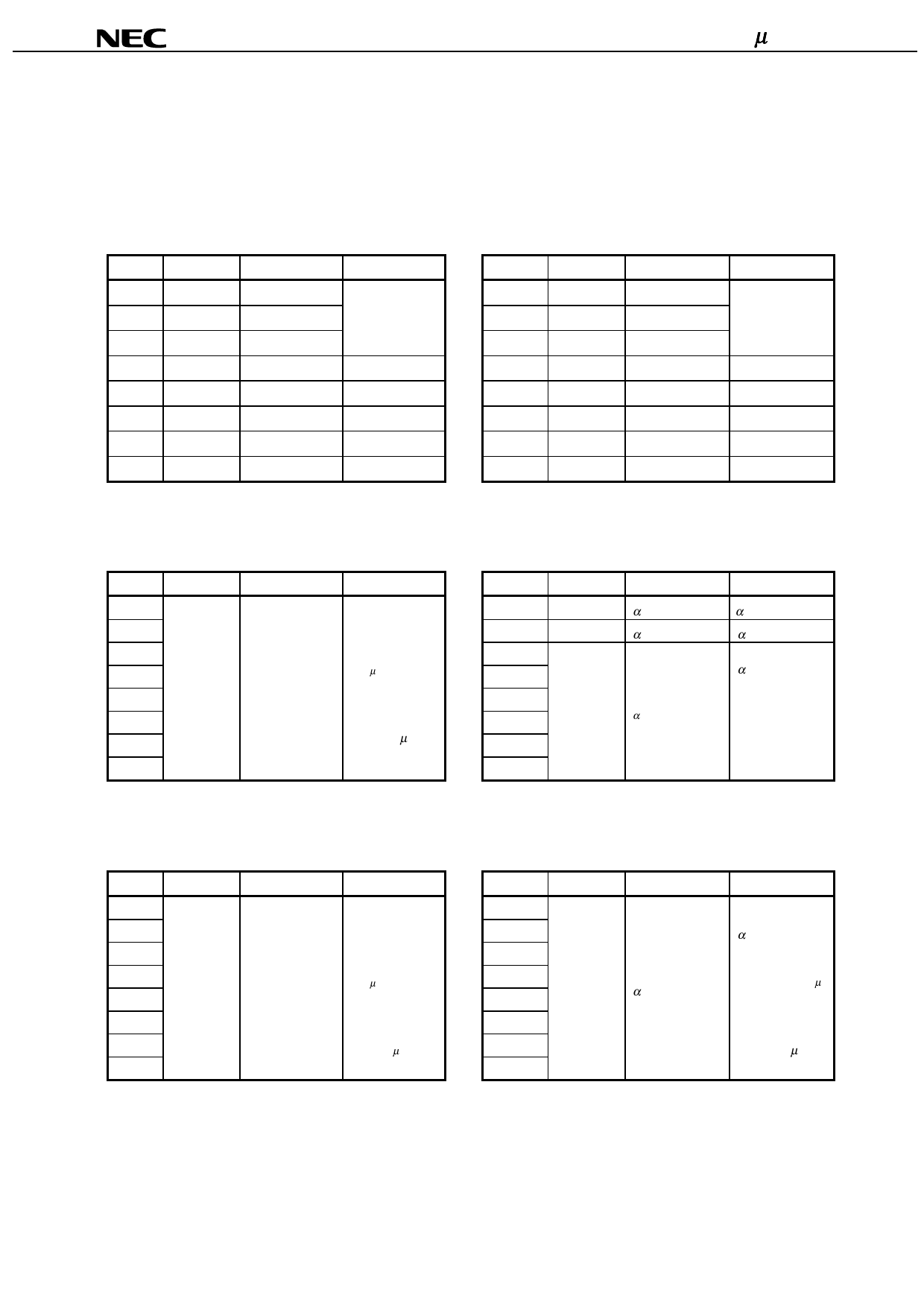
5. INTERFACE (I/F) CIRCUIT DATA CONFIGURATION (fCLK = 4-MHz EXTERNAL CLOCK INPUT)
Input data consists of serial data (8 bytes x 8 bits).
Input serial data with the LSB first, from the 1st byte to 8th byte.
(1) Initial data
<1st byte>
Bit
Data
Function
Setting
D7 1
HEADER DATA2 DATA selection
D6 1
HEADER DATA1
D5 1
HEADER DATA0
D4 0
-
-
D3 1 or 0
EXP3
Hi-Z or L
D2 1 or 0
EXP2
Hi-Z or L
D1 1 or 0
EXP1
Hi-Z or L
D0 1 or 0
EXP0
Hi-Z or L
Remark Hi-Z : High impedance,
L : Low level (current sink)
(2) Standard data
<1st byte>
Bit
Data
Function
D7
0
HEADER DATA2
D6
0
HEADER DATA1
D5
0
HEADER DATA0
D4
0
-
D3
1 or 0
EXP3
D2
1 or 0
EXP2
D1
1 or 0
EXP1
D0
1 or 0
EXP0
Remark Hi-Z : High impedance,
L : Low level (current sink)
Setting
DATA selection
-
Hi-Z or L
Hi-Z or L
Hi-Z or L
Hi-Z or L
<2nd byte>
Bit
Data
Function
Setting
D7
D6
Start point wait
D5
256 µs to 65.28 ms
D4 8-bit data
D3
input Note
First Point Wait Setting
(1 to 255)
D2
∆t = 256 µs
D1
D0
Note Input other than “0”.
<2nd byte>
Bit
Data
Function
Setting
D7
1 or 0
D6
1 or 0
α ROTATION
α ENABLE
α ch CCW/CW
α ch ON/OFF
D5
α ch
D4
D3
6-bit data
Number of
D2
input
α Pulse Number pulses in 1 VD
Setting (0 to 63)
D1
∆n = 4 pulses Note
D0
Note The number of pulses can be varied in 4-pulse
steps.
<3rd byte>
Bit
Data
Function
Setting
D7
D6
Start point drive
D5
wait
D4 8-bit data First Point
256 µs to 65.28 ms
D3
input Note
Magnetize Wait Setting
D2
(1 to 255)
D1
∆t = 256 µs
D0
Note Input other than “0”.
<3rd byte>
Bit
Data
Function
D7
15-bit data
D6
D5
D4
α Pulse Width
D3
Low-order
D2
8-bit data
D1
input
D0
Setting
α ch pulse
cycle
0.25 to 8191.75 µs
Setting
(1 to 32767)
∆t = 0.25 µs
Data Sheet G11594EJ2V0DS00
9
Share Link: 